- 您現(xiàn)在的位置:買賣IC網(wǎng) > PDF目錄16779 > MAX9888EVKIT+ (Maxim Integrated Products)KIT EVALUATION FOR MAX9888 PDF資料下載
參數(shù)資料
| 型號(hào): | MAX9888EVKIT+ |
| 廠商: | Maxim Integrated Products |
| 文件頁數(shù): | 112/115頁 |
| 文件大小: | 0K |
| 描述: | KIT EVALUATION FOR MAX9888 |
| 產(chǎn)品培訓(xùn)模塊: | Lead (SnPb) Finish for COTS Obsolescence Mitigation Program |
| 標(biāo)準(zhǔn)包裝: | 1 |
| 系列: | DirectDrive®, FLEXSOUND™ |
| 相關(guān)產(chǎn)品: | MAX9888EWY+T-ND - IC CODEC AUDIO FLEXSOUND 63WLP |
第1頁第2頁第3頁第4頁第5頁第6頁第7頁第8頁第9頁第10頁第11頁第12頁第13頁第14頁第15頁第16頁第17頁第18頁第19頁第20頁第21頁第22頁第23頁第24頁第25頁第26頁第27頁第28頁第29頁第30頁第31頁第32頁第33頁第34頁第35頁第36頁第37頁第38頁第39頁第40頁第41頁第42頁第43頁第44頁第45頁第46頁第47頁第48頁第49頁第50頁第51頁第52頁第53頁第54頁第55頁第56頁第57頁第58頁第59頁第60頁第61頁第62頁第63頁第64頁第65頁第66頁第67頁第68頁第69頁第70頁第71頁第72頁第73頁第74頁第75頁第76頁第77頁第78頁第79頁第80頁第81頁第82頁第83頁第84頁第85頁第86頁第87頁第88頁第89頁第90頁第91頁第92頁第93頁第94頁第95頁第96頁第97頁第98頁第99頁第100頁第101頁第102頁第103頁第104頁第105頁第106頁第107頁第108頁第109頁第110頁第111頁當(dāng)前第112頁第113頁第114頁第115頁
Stereo Audio CODEC
with FlexSound Technology
MAX9888
96
Alternative approaches to eliminating the output-cou-
pling capacitors involve biasing the headphone return
(sleeve) to the DC bias voltage of the headphone ampli-
fiers. This method raises some issues:
U
The sleeve is typically grounded to the chassis. Using
the midrail biasing approach, the sleeve must be
isolated from system ground, complicating product
design.
U
During an ESD strike, the amplifier’s ESD structures
are the only path to system ground. Thus, the ampli-
fier must be able to withstand the full energy from an
ESD strike.
U
When using the headphone jack as a line out to other
equipment, the bias voltage on the sleeve may con-
flict with the ground potential from other equipment,
resulting in possible damage to the amplifiers.
The IC features a low-noise charge pump to generate
a negative supply for the headphone amplifier. The
nominal switching frequency is well beyond the audio
range, and thus does not interfere with audio signals.
The switch drivers feature a controlled switching speed
that minimizes noise generated by turn-on and turn-off
transients. By limiting the switching speed of the charge
pump, the di/dt noise caused by the parasitic trace
inductance is minimized. The charge pump is active only
in headphone modes.
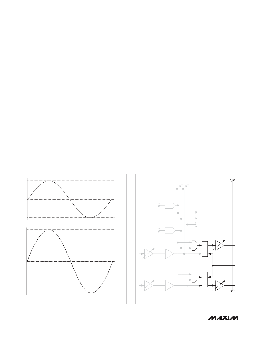
To reduce audible noise at the outputs, the IC’s head-
phone amplifier includes headphone ground sensing.
Connect the sense line (HPSNS) to the ground terminal
of the device’s headphone jack. Any noise present at
the headphone ground is then added to the headphone
output. The result is elimination of this noise from the
audible output. If ground sensing is not required, con-
nect HPSNS directly to ground. Figure 30 shows a block
diagram of the headphone output section including the
headphone sense function.
Headphone Output Mixers
The IC’s headphone amplifier accepts input from the
stereo DAC and the line inputs. The output of the left and
right DAC cannot be mixed at the headphone mixer. Use
MIXDAL/MIXDAR to mix the left and right audio channels
before conversion.
Figure 29. Traditional Amplifier Output vs. DirectDrive Output
Figure 30. Headphone Amplifier Block Diagram
VDD
VDD/2
GND
CONVENTIONAL AMPLIFIER BIASING SCHEME
DirectDrive AMPLIFIER BIASING SCHEME
+VDD
GND
-VDD
(VSS)
MIXHPL
MIXHPR
MIX
PGAOUT2:
0dB TO -23dB
HPVOLL:
+3dB TO -67dB
HPVOLR:
+3dB TO -67dB
PREOUT2
+9dB
PGAOUT1:
0dB TO -23dB
DAREN
HPL
HPSNS
HPLEN
HPREN
HPR
PREOUT1
+9dB
DACR
DALEN
DACL
相關(guān)PDF資料 |
PDF描述 |
|---|---|
| H3AAH-3418G | IDC CABLE - HSC34H/AE34G/HSC34H |
| EBM22DRAI | CONN EDGECARD 44POS R/A .156 SLD |
| RNF-100-1/8-GN-STK | HEAT SHRINK TUBING |
| RSC06DREF-S13 | CONN EDGECARD 12POS .100 EXTEND |
| GEC26DRXN-S734 | CONN EDGECARD 52POS DIP .100 SLD |
相關(guān)代理商/技術(shù)參數(shù) |
參數(shù)描述 |
|---|---|
| MAX9888EVKIT+ | 功能描述:音頻 IC 開發(fā)工具 MAX9888 Eval Kit RoHS:否 制造商:Texas Instruments 產(chǎn)品:Evaluation Kits 類型:Audio Amplifiers 工具用于評(píng)估:TAS5614L 工作電源電壓:12 V to 38 V |
| MAX9888EWY+T | 功能描述:接口—CODEC Stereo Audio CODEC RoHS:否 制造商:Texas Instruments 類型: 分辨率: 轉(zhuǎn)換速率:48 kSPs 接口類型:I2C ADC 數(shù)量:2 DAC 數(shù)量:4 工作電源電壓:1.8 V, 2.1 V, 2.3 V to 5.5 V 最大工作溫度:+ 85 C 安裝風(fēng)格:SMD/SMT 封裝 / 箱體:DSBGA-81 封裝:Reel |
| MAX9889EWO+T | 功能描述:接口—CODEC RoHS:否 制造商:Texas Instruments 類型: 分辨率: 轉(zhuǎn)換速率:48 kSPs 接口類型:I2C ADC 數(shù)量:2 DAC 數(shù)量:4 工作電源電壓:1.8 V, 2.1 V, 2.3 V to 5.5 V 最大工作溫度:+ 85 C 安裝風(fēng)格:SMD/SMT 封裝 / 箱體:DSBGA-81 封裝:Reel |
| MAX988ESA | 功能描述:校驗(yàn)器 IC Single uPower Comparator RoHS:否 制造商:STMicroelectronics 產(chǎn)品: 比較器類型: 通道數(shù)量: 輸出類型:Push-Pull 電源電壓-最大:5.5 V 電源電壓-最小:1.1 V 補(bǔ)償電壓(最大值):6 mV 電源電流(最大值):1350 nA 響應(yīng)時(shí)間: 最大工作溫度:+ 125 C 安裝風(fēng)格:SMD/SMT 封裝 / 箱體:SC-70-5 封裝:Reel |
| MAX988ESA+ | 功能描述:校驗(yàn)器 IC Single uPower Comparator RoHS:否 制造商:STMicroelectronics 產(chǎn)品: 比較器類型: 通道數(shù)量: 輸出類型:Push-Pull 電源電壓-最大:5.5 V 電源電壓-最小:1.1 V 補(bǔ)償電壓(最大值):6 mV 電源電流(最大值):1350 nA 響應(yīng)時(shí)間: 最大工作溫度:+ 125 C 安裝風(fēng)格:SMD/SMT 封裝 / 箱體:SC-70-5 封裝:Reel |
發(fā)布緊急采購,3分鐘左右您將得到回復(fù)。