- 您現(xiàn)在的位置:買賣IC網(wǎng) > PDF目錄385555 > MAX9180EXT-T (MAXIM INTEGRATED PRODUCTS INC) 400Mbps, Low-Jitter, Low-Noise LVDS Repeater in an SC70 Package PDF資料下載
參數(shù)資料
| 型號(hào): | MAX9180EXT-T |
| 廠商: | MAXIM INTEGRATED PRODUCTS INC |
| 元件分類: | 通用總線功能 |
| 英文描述: | 400Mbps, Low-Jitter, Low-Noise LVDS Repeater in an SC70 Package |
| 中文描述: | LINE TRANSCEIVER, PDSO6 |
| 封裝: | SC-70, 6 PIN |
| 文件頁(yè)數(shù): | 5/9頁(yè) |
| 文件大小: | 255K |
| 代理商: | MAX9180EXT-T |

Detailed Description
The LVDS interface standard is a signaling method
intended for point-to-point communication over a con-
trolled-impedance medium, as defined by the ANSI/
TIA/EIA-644 and IEEE 1596.3 standards. The LVDS
standard uses a lower voltage swing than other com-
mon communication standards, achieving higher data
rates with reduced power consumption while reducing
EMI emissions and system susceptibility to noise.
The MAX9180 is a 400Mbps LVDS repeater intended
for high-speed, point-to-point, low-power applications.
The MAX9180 accepts an LVDS input and reproduces
an LVDS signal at the output. This device is capable of
detecting differential signals as low as 50mV and as
high as 1.2V within a 0 to 2.4V input voltage range. The
LVDS standard specifies an input voltage range of 0 to
2.4V referenced to ground.
Fail-Safe
Fail-safe is a feature that puts the output in a known
logic state (differential high) under certain fault condi-
tions. The MAX9180 outputs are differential high when
the inputs are undriven and open, terminated, or shorted
(Table 1).
M
400Mbps, Low-Jitter, Low-Noise LVDS
Repeater in an SC70 Package
_______________________________________________________________________________________
5
400
450
500
550
600
650
700
750
800
-40
-15
10
35
60
85
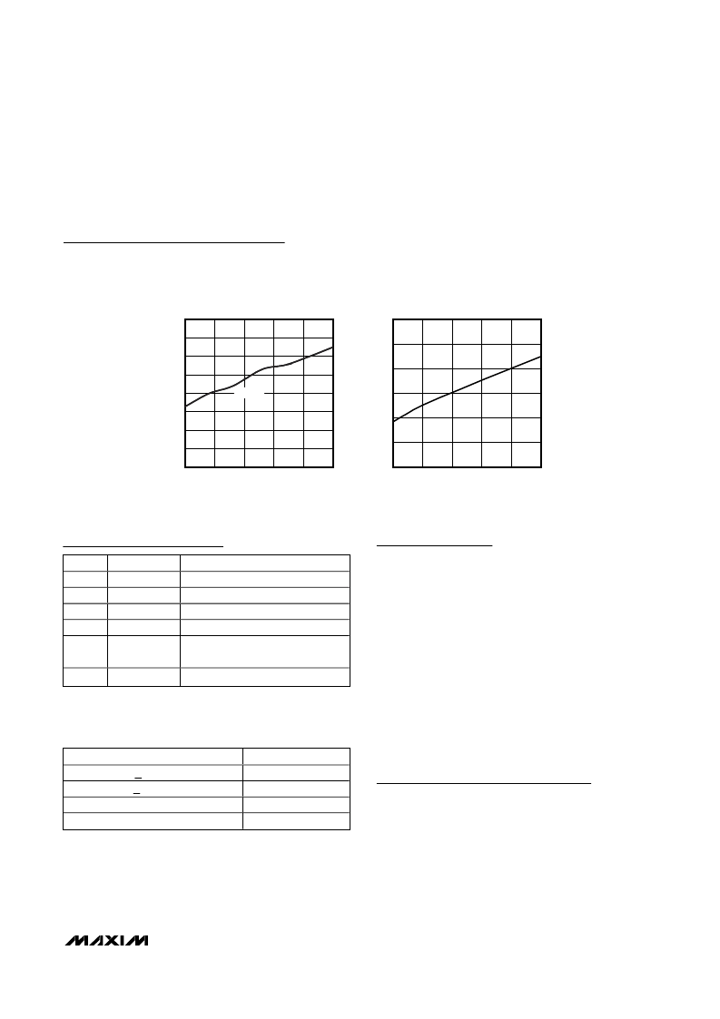
TRANSITION TIME
VS.
TEMPERATURE
M
TEMPERATURE (
°
C)
T
t
TLH
, t
THL
0
200
100
400
300
500
600
25
150
DIFFERENTIAL OUTPUT VOLTAGE
VS.
LOAD RESISTOR
M
LOAD RESISTOR (
)
D
75
50
100
125
Typical Operating Characteristics (continued)
(V
CC
= 3.3V, R
L
= 100
±1%, C
L
= 10pF,
|
V
ID
|
= 0.2V, V
CM
= 1.2V, T
A
= +25°C, unless otherwise noted. Signal generator output:
frequency = 200MHz, 50% duty cycle, R
O
= 50
, t
R
= 1.5ns, and t
F
= 1.5ns (0% to 100%), unless otherwise noted.)
Pin Description
PIN
1
2
3
4
NAME
OUT-
GND
IN-
IN+
FUNCTION
Inverting LVDS Output
Ground
Inverting LVDS Input
Noninverting LVDS Input
5
V
CC
Power Supply. Bypass V
CC
to GND
with a 0.01μF ceramic capacitor.
6
OUT+
Noninverting LVDS Output
INPUT, V
ID
>50mV
<-50mV
50mV
>
V
ID
>
-50mV
Undriven open, short, or terminated
OUTPUT, V
OD
High
Low
Indeterminate
High
Note:
V
ID
= (IN+ - IN-), V
OD
= (OUT+ - OUT-)
High = 450mV
≥
V
OD
≥
250mV
Low = -250mV
≥
V
OD
≥
-450mV
Table 1. Function Table for LVDS Fail-Safe
Input (Figure 2)
相關(guān)PDF資料 |
PDF描述 |
|---|---|
| MAX9205EVKIT | Evaluation Kit for the MAX9205/MAX9206/MAX9207/MAX9208 |
| MAX9209 | Programmable DC-Balanced 21-Bit Serializers |
| MAX9211 | Programmable DC-Balanced 21-Bit Serializers |
| MAX9213 | Programmable DC-Balanced 21-Bit Serializers |
| MAX9215 | Programmable DC-Balanced 21-Bit Serializers |
相關(guān)代理商/技術(shù)參數(shù) |
參數(shù)描述 |
|---|---|
| MAX9181 | 制造商:MAXIM 制造商全稱:Maxim Integrated Products 功能描述:Low-Jitter.Low-Noise LVPECL-to-LVDS Level Translator in an SC70 Package |
| MAX9181EXT | 制造商:Maxim Integrated Products 功能描述:LOW-JITTER, LOW-NOISE LVPECL-TO-LVDS LEVEL TR - Cut Tape Product |
| MAX9181EXT-T | 制造商:Maxim Integrated Products 功能描述:LOW-JITTER, LOW-NOISE LVPECL-TO-LVDS LEVEL TR - Tape and Reel |
| MAX918ESA | 功能描述:校驗(yàn)器 IC RoHS:否 制造商:STMicroelectronics 產(chǎn)品: 比較器類型: 通道數(shù)量: 輸出類型:Push-Pull 電源電壓-最大:5.5 V 電源電壓-最小:1.1 V 補(bǔ)償電壓(最大值):6 mV 電源電流(最大值):1350 nA 響應(yīng)時(shí)間: 最大工作溫度:+ 125 C 安裝風(fēng)格:SMD/SMT 封裝 / 箱體:SC-70-5 封裝:Reel |
| MAX918ESA+ | 功能描述:校驗(yàn)器 IC 1.8V nPower Comparator RoHS:否 制造商:STMicroelectronics 產(chǎn)品: 比較器類型: 通道數(shù)量: 輸出類型:Push-Pull 電源電壓-最大:5.5 V 電源電壓-最小:1.1 V 補(bǔ)償電壓(最大值):6 mV 電源電流(最大值):1350 nA 響應(yīng)時(shí)間: 最大工作溫度:+ 125 C 安裝風(fēng)格:SMD/SMT 封裝 / 箱體:SC-70-5 封裝:Reel |
發(fā)布緊急采購(gòu),3分鐘左右您將得到回復(fù)。