- 您現(xiàn)在的位置:買賣IC網(wǎng) > PDF目錄383506 > MAX805TMJA (MAXIM INTEGRATED PRODUCTS INC) Octal Bus Transceivers With 3-State Outputs 20-CDIP -55 to 125 PDF資料下載
參數(shù)資料
| 型號: | MAX805TMJA |
| 廠商: | MAXIM INTEGRATED PRODUCTS INC |
| 元件分類: | 電源管理 |
| 英文描述: | Octal Bus Transceivers With 3-State Outputs 20-CDIP -55 to 125 |
| 中文描述: | 1-CHANNEL POWER SUPPLY MANAGEMENT CKT, CDIP8 |
| 封裝: | 0.300 INCH, CERDIP-8 |
| 文件頁數(shù): | 2/12頁 |
| 文件大小: | 98K |
| 代理商: | MAX805TMJA |
M
Mic roproc essor S upervisory Circ uits
2
_______________________________________________________________________________________
Terminal Voltage (with respect to GND)
V
CC
............................................... -0.3V to 6.0V
V
.............................................. -0.3V to 6.0V
All Other Inputs (Note 1) ................ -0.3V to (V
CC
+ 0.3V)
Input Current
V
CC
...................................................... 200mA
V
..................................................... 50mA
GND ...................................................... 20mA
Output Current
V
................... Short-Circuit Protected for up to 10sec
All Other Outputs ........................................ 20mA
Rate of Rise, V
, V
................................ 100V/μs
Continuous Power Dissipation
Plastic DIP (derate 9.09mW/°C above +70°C) ........ 727mW
SO (derate 5.88mW/°C above +70°C) ................ 471mW
CERDIP (derate 8.00mW/°C above +70°C) ........... 640mW
Operating Temperature Ranges:
MAX69_AC_ _, MAX80_ _ C_ _ .................. 0°C to +70°C
MAX69_AE_ _, MAX80_ _ E_ _ ................ -40°C to +85°C
MAX69_AMJ A, MAX805LMJ A................ -55°C to +125°C
Storage Temperature Range .................. -65°C to +160°C
Lead Temperature (soldering, 10sec) .................. +300°C
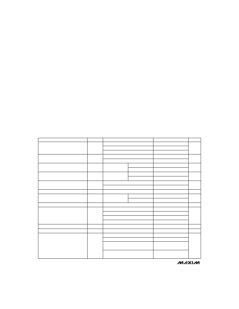
ELECTRICAL CHARACTERISTICS
(V
CC
= 4.75V to 5.5V for MAX690A/MAX802L/MAX805L, V
CC
= 4.5V to 5.5V for MAX692A/MAX802M, V
BATT
= 2.8V,
T
A
= T
MIN
to T
MAX
, unless otherwise noted.)
PARAMETER
SYMBOL
CONDITIONS
MAX69_AC, MAX802_C
MAX805LC
MAX69_AE/M, MAX80_ _E
MAX69_AC, MAX802_C
MAX69_AE/M, MAX802_E, MAX805LE/M
I
SUPPLY
in Battery-Backup Mode
(Excluding I
OUT
)
V
BATT
= 2.8V
Stresses beyond those listed under "Absolute Maximum Ratings may cause permanent damage to the device. These are stress ratings only, and functional
operation of the device at these or any other conditions beyond those indicated in the operational sections of the specifications is not implied. Exposure to
absolute maximum rating conditions for extended periods may affect device reliability.
MIN
1.0
1.1
TYP
MAX
5.5
5.5
UNITS
Operating Voltage Range,
V
CC
, V
BATT
(Note 2)
V
1.2
5.5
350
500
1.0
5.0
0.02
0.02
Supply Current (Excluding I
OUT
)
I
SUPPLY
200
200
0.05
μA
V
CC
= 0V,
5.5V > V
>
V
BATT
+0.2V
I
OUT
= 5mA
I
OUT
= 50mA
-0.1
-1.0
μA
V
OUT
Output
V
CC
- 0.05 V
CC
- 0.025
V
CC
- 0.5
V
BATT
- 0.1 V
BATT
- 0.02
V
ABSOLUTE MAXIMUM RATINGS
Note 1:
The input voltage limits on PFI and WDI may be exceeded if the current into these pins is limited to less than 10mA.
V
BATT
Standby Current (Note 3)
V
CC
- 0.25
V
OUT
in Battery-Backup Mode
Battery Switch Threshold, V
CC
to V
BATT
I
OUT
= 250μA, V
CC
< V
BATT
- 0.2V
V
V
CC
< V
RT
20
-20
40
4.65
mV
μA
T
A
= +25°C
T
A
= T
MIN
to T
MAX
T
A
= +25°C
T
A
= T
MIN
to T
MAX
Power-up
Power-down
Battery Switchover Hysteresis
mV
Reset Threshold
V
RT
MAX690A, MAX802L, MAX805L
MAX692A, MAX802M
MAX802L, T
A
= +25°C, V
CC
falling
MAX802M, T
A
= +25°C, V
CC
falling
V
4.25
4.55
4.30
4.40
4.50
4.70
4.45
Reset Threshold Hysteresis
Reset Pulse Width
40
200
mV
ms
t
RS
140
280
RESET
Output Voltage
I
SOURCE
= 800μA
I
SINK
= 3.2mA
MAX69_AC, MAX802_C, V
CC
= 1.0V
I
SINK
= 50μA
MAX69_AE/M, MAX802_E,
V
CC
= 1.2V, I
SINK
= 100μA
V
CC
- 1.5
V
0.4
0.3
0.3
4.50
4.75
相關(guān)PDF資料 |
PDF描述 |
|---|---|
| MAX805RESA | 3.0V/3.3V Microprocessor Supervisory Circuits |
| MAX805RCSA | CANCA02COME36A35SBF80 |
| MAX808LMJA | Interface IC |
| MAX808 | 8-Pin レP Supervisory Circuits with 【1.5eset Accuracy |
| MAX801L-MAX808N | 5015 RR 3#8 SKT RECP |
相關(guān)代理商/技術(shù)參數(shù) |
參數(shù)描述 |
|---|---|
| MAX806 | 制造商:MAXIM 制造商全稱:Maxim Integrated Products 功能描述:Microprocessor Supervisory Circuits |
| MAX806_C/D | 制造商:MAXIM 制造商全稱:Maxim Integrated Products 功能描述:3.0V/3.3V Microprocessor Supervisory Circuits |
| MAX806_CPA | 制造商:MAXIM 制造商全稱:Maxim Integrated Products 功能描述:3.0V/3.3V Microprocessor Supervisory Circuits |
| MAX806_CSA | 制造商:MAXIM 制造商全稱:Maxim Integrated Products 功能描述:3.0V/3.3V Microprocessor Supervisory Circuits |
| MAX806_EPA | 制造商:MAXIM 制造商全稱:Maxim Integrated Products 功能描述:3.0V/3.3V Microprocessor Supervisory Circuits |
發(fā)布緊急采購,3分鐘左右您將得到回復(fù)。