- 您現(xiàn)在的位置:買賣IC網(wǎng) > PDF目錄3767 > MAX7324ATG+T (Maxim Integrated Products)IC I/O EXPANDER I2C 8B 24TQFN-EP PDF資料下載
參數(shù)資料
| 型號: | MAX7324ATG+T |
| 廠商: | Maxim Integrated Products |
| 文件頁數(shù): | 19/20頁 |
| 文件大小: | 0K |
| 描述: | IC I/O EXPANDER I2C 8B 24TQFN-EP |
| 產(chǎn)品培訓(xùn)模塊: | Lead (SnPb) Finish for COTS Obsolescence Mitigation Program |
| 標(biāo)準(zhǔn)包裝: | 2,500 |
| 接口: | I²C |
| 輸入/輸出數(shù): | 8 |
| 中斷輸出: | 是 |
| 頻率 - 時(shí)鐘: | 400kHz |
| 電源電壓: | 1.71 V ~ 5.5 V |
| 工作溫度: | -40°C ~ 125°C |
| 安裝類型: | 表面貼裝 |
| 封裝/外殼: | 24-WFQFN 裸露焊盤 |
| 供應(yīng)商設(shè)備封裝: | 24-TQFN-EP(4x4) |
| 包裝: | 帶卷 (TR) |
| 包括: | POR |

MAX7324
I2C Port Expander with Eight Push-Pull Outputs
and Eight Inputs
8
_______________________________________________________________________________________
address selection determines which inputs have
pullups applied. However, at power-up, the I2C SDA
and SCL bus interface lines are high impedance at the
inputs of every device (master or slave) connected to
the bus, including the MAX7324. This is guaranteed as
part of the I2C specification. Therefore, address inputs
AD0 and AD2 that are connected to SDA or SCL during
power-up appear to be connected to V+. The pullup
selection logic uses AD0 to select whether pullups are
enabled for ports I0–I3, and uses AD2 to select whether
pullups are enabled for ports I4–I7. The rule is that a
logic-high SDA, or SCL connection selects the pullups,
while a logic-low deselects the pullups (Table 2). The
pullup configuration is correct on power-up for a stan-
dard I2C configuration, where SDA and SCL are pulled
up to V+ by the external I2C pullups.
There are circumstances where the assumption that
SDA = SCL = V+ on power-up is not true—for example,
in applications in which there is legitimate bus activity
during power-up. Also, if SDA and SCL are terminated
with pullup resistors to a different supply voltage than
the MAX7324’s supply voltage, and if that pullup supply
rises later than the MAX7324’s supply, then SDA or
SCL may appear at power-up to be connected to GND.
In such applications, use the four address combina-
tions that are selected by connecting address inputs
AD0 and AD2 to V+ or GND (shown in
bold in Tables 2
and 3). These selections are guaranteed to be correct
at power-up, independent of SDA and SCL behavior. If
one of the other 12 address combinations is used, an
unexpected combination of pullups might be asserted
until the first I2C transmission (to any device, not neces-
sarily the MAX7324) is put on the bus.
Port Inputs
Port inputs switch at CMOS logic levels as determined
by the expander’s supply voltage, and are overvoltage
tolerant to +6V, independent of the device’s supply
voltage.
Port-Input Transition Detection
All eight input ports are monitored for changes since
the expander was last accessed through the serial
interface. The state of the input ports is stored in an
internal “snapshot” register for transition monitoring.
The snapshot is continuously compared with the actual
input conditions, and if a change is detected for any
port input, then an internal transition flag is set for that
port. The eight port inputs are sampled (internally
latched into the snapshot register) and the old transi-
tion flags cleared during the I2C acknowledge of every
MAX7324 read and write access. The previous port
transition flags are read through the serial interface as
the second byte of a 2-byte read sequence.
PIN CONNECTION
DEVICE ADDRESS
40k
INPUT PULLUP ENABLED
AD2
AD0
A6
A5
A4
A3
A2
A1
A0
I7
I6
I5
I4
I3
I2
I1
I0
SCL
GND
1100
000
YYYY
——
—
SCL
V+
1100
001
YYYYY
YYY
SCL
1100
010
YYYYY
YYY
SCL
SDA
1100
011
YYYYY
YYY
SDA
GND
1100
100
YYYY
——
—
SDA
V+
1100
101
YYYYY
YYY
SDA
SCL
1100
110
YYYYY
YYY
SDA
1100
111
YYYYY
YYY
GND
1101
000
—————
——
—
GND
V+
1101
001
————
Y
YYY
GND
SCL
1101
010
————
Y
YYY
GND
SDA
1101
011
————
Y
YYY
V+
GND
1101
100
YYYY
——
—
V+
1101
101
YYYYY
YYY
V+
SCL
1101
110
YYYYY
YYY
V+
SDA
1101
111
YYYYY
YYY
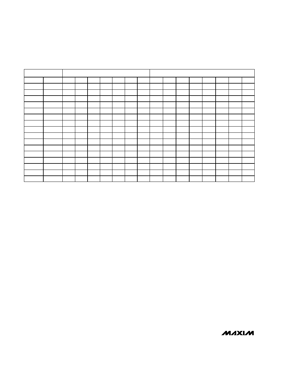
Table 2. MAX7324 Address Map for Inputs I0–I7
相關(guān)PDF資料 |
PDF描述 |
|---|---|
| XR21V1410IL16-F | IC UART FIFO USB SGL 16QFN |
| XR16L580IL-F | IC UART FIFO 16BYTE 32QFN |
| XR16M681IL24-F | IC UART FIFO 64B 24QFN |
| XR16M681IB25-F | IC UART FIFO 64B 25BGA |
| ST16C550IJ44-F | IC UART FIFO 16B SGL 44PLCC |
相關(guān)代理商/技術(shù)參數(shù) |
參數(shù)描述 |
|---|---|
| MAX7324EVCMAXQU+ | 功能描述:界面開發(fā)工具 Maxim Evaluation System RoHS:否 制造商:Bourns 產(chǎn)品:Evaluation Boards 類型:RS-485 工具用于評估:ADM3485E 接口類型:RS-485 工作電源電壓:3.3 V |
| MAX7324EVKIT+ | 功能描述:界面開發(fā)工具 Evaluation Kit/Evaluation System for the MAX7324 RoHS:否 制造商:Bourns 產(chǎn)品:Evaluation Boards 類型:RS-485 工具用于評估:ADM3485E 接口類型:RS-485 工作電源電壓:3.3 V |
| MAX7325 | 制造商:MAXIM 制造商全稱:Maxim Integrated Products 功能描述:I2C Port Expander with 8 Push-Pull and 8 Open-Drain I/Os |
| MAX7325_12 | 制造商:MAXIM 制造商全稱:Maxim Integrated Products 功能描述:I2C Port Expander with 8 Push-Pull and 8 Open-Drain I/Os |
| MAX7325AEG | 功能描述:接口-I/O擴(kuò)展器 I2C Port Expander w/8 P-P Out & 8 I/O RoHS:否 制造商:NXP Semiconductors 邏輯系列: 輸入/輸出端數(shù)量: 最大工作頻率:100 kHz 工作電源電壓:1.65 V to 5.5 V 工作溫度范圍:- 40 C to + 85 C 安裝風(fēng)格:SMD/SMT 封裝 / 箱體:HVQFN-16 封裝:Reel |
發(fā)布緊急采購,3分鐘左右您將得到回復(fù)。