- 您現(xiàn)在的位置:買賣IC網(wǎng) > PDF目錄383443 > MAX5895EGK (MAXIM INTEGRATED PRODUCTS INC) 16-Bit, 500Msps Interpolating and Modulating Dual DAC with CMOS Inputs PDF資料下載
參數(shù)資料
| 型號: | MAX5895EGK |
| 廠商: | MAXIM INTEGRATED PRODUCTS INC |
| 元件分類: | DAC |
| 英文描述: | 16-Bit, 500Msps Interpolating and Modulating Dual DAC with CMOS Inputs |
| 中文描述: | PARALLEL, WORD INPUT LOADING, 0.011 us SETTLING TIME, 16-BIT DAC, QCC68 |
| 封裝: | 10 X 10 MM, MO-220, QFN-68 |
| 文件頁數(shù): | 25/32頁 |
| 文件大小: | 807K |
| 代理商: | MAX5895EGK |
第1頁第2頁第3頁第4頁第5頁第6頁第7頁第8頁第9頁第10頁第11頁第12頁第13頁第14頁第15頁第16頁第17頁第18頁第19頁第20頁第21頁第22頁第23頁第24頁當(dāng)前第25頁第26頁第27頁第28頁第29頁第30頁第31頁第32頁
their default values in Table 2. During power-on,
RESET
must be held low until all power supplies have stabi-
lized. Alternately, programming bit 5 of address 00h to
a logic-high also resets the MAX5895 after power-up.
Power-Down Mode
The MAX5895 features three power-saving modes.
Each DAC can be individually powered down through
bits 2 and 3 of address 00h. The interpolation filters can
also be powered down through bit 4 of address 00h,
preserving the output level of each DAC (the DACs
remain powered). Powering down both DACs will auto-
matically put the MAX5895 into full power-down, includ-
ing the interpolation filters.
Applications Information
Frequency Planning
System designers need to take the DAC into account
during frequency planning for high-performance appli-
cations. Proper frequency planning can ensure that
optimal system performance is achieved. The
MAX5895 is designed to deliver excellent dynamic per-
formance across wide bandwidths, as required for
communication systems and, in particular, for multicar-
rier applications. As with all DACs, some combinations
of output frequency and update rate produce better
performance than others.
Harmonics are often folded down into the band of inter-
est. Specifically, if the DAC outputs a frequency close
to f
S
/ N, the Mth harmonic of the output signal will be
aliased down to:
f
f
M x f
S
=
Thus, if N
≈
(M + 1), the Mth harmonic will be close to
the output frequency. SFDR performance of a current-
steering DAC is often dominated by third-order har-
monic distortion. If this is a concern, placing the output
signal at a different frequency other than f
S
/ 4 should
be considered.
Common to interpolating DACs are images near the
divided clocks. In a DAC configured for 4x interpolation
this applies to images around f
S
/ 4 and f
S
/ 2. In a DAC
configured for 8x interpolation this applies to images
around f
S
/ 8, f
S
/ 4, and f
S
/ 2. Most of these images
are not part of the in-band (0 to f
DATA
/ 2) SFDR specifi-
cation, though they are a consideration for out-of-band
(f
DATA
/ 2 - f
DAC
/ 2) SFDR and may depend on the
relationship of the DATACLK to DAC update clock (see
the
Data Clock
section). When specifying the output
reconstruction filter for other than baseband signals,
these images should not be ignored.
Data Clock
The MAX5895 features synchronizers that allow for
arbitrary phase alignment between DATACLK and
CLKP/CLKN. The DATACLK causes internal switching
in the MAX5895 and the phase between DATACLK
(input mode) to CLKP/CLKN will influence the images
at DATACLK. Optimum image rejection is achieved
when DATACLK transitions are aligned with the falling
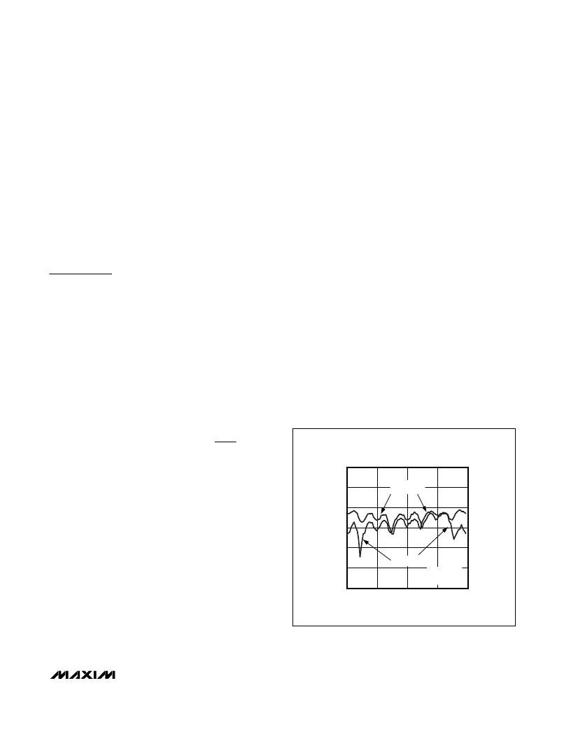
edge of CLKP. Figure 14 shows the image level near
DATACLK as a function of the DATACLK (input mode)
to CLKP/CLKN phase at 500Msps, 4x interpolation for a
10MHz, -6dBFS output signal.
Clock Interface
The MAX5895 features a flexible differential clock input
(CLKP, CLKN) with a separate supply (AV
CLK
) to
achieve optimum jitter performance. It uses an ultra-low
jitter clock to achieve the required noise density. Clock
jitter must be less than 0.5ps
RMS
to meet the specified
noise density. For that reason, the CLKP/CLKN input
source must be designed carefully. The differential
clock (CLKN and CLKP) input can be driven from a sin-
gle-ended or a differential clock source. Differential
clock drive is required to achieve the best dynamic
performance from the DAC. For single-ended opera-
tion, drive CLKP with a low noise source and bypass
CLKN to GND with a 0.1μF capacitor.
The CLKP and CLKN pins are internally biased to
AV
CLK
/ 2. This allows the user to AC-couple clock
f
N M
N
OUT
S
=
M
16-Bit, 500Msps Interpolating and Modulating
Dual DAC with CMOS Inputs
______________________________________________________________________________________
25
Figure 14. Effect of CLKP/CLKN to DATACLK Phase on f
S
/ 4
Images
f
S
/ 4 IMAGES vs. CLKP/CLKN to DATACLK DELAY
f
DATA
= 125MWps, 4x INTERPOLATION
-50
CLKP/CLKN DELAY (ns)
I
6.0
4.0
2.0
-100
-90
-80
-70
-60
-110
0
8.0
f
S
/ 4 - f
OUT
f
OUT
= 10MHz
A
OUT
= -6dBFS
f
S
/ 4 + f
OUT
相關(guān)PDF資料 |
PDF描述 |
|---|---|
| MAX5901ACEUT | Analog IC |
| MAX5927 | Low-Voltage. Quad. Hot-Swap Controllers/Power Sequencers |
| MAX5929 | Low-Voltage. Quad. Hot-Swap Controllers/Power Sequencers |
| MAX5930 | Low-Voltage. Triple. Hot-Swap Controllers/Power Sequencers/Voltage Trackers |
| MAX5931 | Low-Voltage. Triple. Hot-Swap Controllers/Power Sequencers/Voltage Trackers |
相關(guān)代理商/技術(shù)參數(shù) |
參數(shù)描述 |
|---|---|
| MAX5895EGK+D | 功能描述:數(shù)模轉(zhuǎn)換器- DAC 16-Bit 2Ch 500Msps DAC RoHS:否 制造商:Texas Instruments 轉(zhuǎn)換器數(shù)量:1 DAC 輸出端數(shù)量:1 轉(zhuǎn)換速率:2 MSPs 分辨率:16 bit 接口類型:QSPI, SPI, Serial (3-Wire, Microwire) 穩(wěn)定時間:1 us 最大工作溫度:+ 85 C 安裝風(fēng)格:SMD/SMT 封裝 / 箱體:SOIC-14 封裝:Tube |
| MAX5895EGK+TD | 功能描述:數(shù)模轉(zhuǎn)換器- DAC 16-Bit 2Ch 500Msps DAC RoHS:否 制造商:Texas Instruments 轉(zhuǎn)換器數(shù)量:1 DAC 輸出端數(shù)量:1 轉(zhuǎn)換速率:2 MSPs 分辨率:16 bit 接口類型:QSPI, SPI, Serial (3-Wire, Microwire) 穩(wěn)定時間:1 us 最大工作溫度:+ 85 C 安裝風(fēng)格:SMD/SMT 封裝 / 箱體:SOIC-14 封裝:Tube |
| MAX5895EGK-D | 功能描述:數(shù)模轉(zhuǎn)換器- DAC RoHS:否 制造商:Texas Instruments 轉(zhuǎn)換器數(shù)量:1 DAC 輸出端數(shù)量:1 轉(zhuǎn)換速率:2 MSPs 分辨率:16 bit 接口類型:QSPI, SPI, Serial (3-Wire, Microwire) 穩(wěn)定時間:1 us 最大工作溫度:+ 85 C 安裝風(fēng)格:SMD/SMT 封裝 / 箱體:SOIC-14 封裝:Tube |
| MAX5895EGK-TD | 功能描述:數(shù)模轉(zhuǎn)換器- DAC RoHS:否 制造商:Texas Instruments 轉(zhuǎn)換器數(shù)量:1 DAC 輸出端數(shù)量:1 轉(zhuǎn)換速率:2 MSPs 分辨率:16 bit 接口類型:QSPI, SPI, Serial (3-Wire, Microwire) 穩(wěn)定時間:1 us 最大工作溫度:+ 85 C 安裝風(fēng)格:SMD/SMT 封裝 / 箱體:SOIC-14 封裝:Tube |
| MAX5895EVCMOD2 | 功能描述:數(shù)模轉(zhuǎn)換器- DAC Evaluation Kit for the MAX5893/MAX5894/MAX5895 RoHS:否 制造商:Texas Instruments 轉(zhuǎn)換器數(shù)量:1 DAC 輸出端數(shù)量:1 轉(zhuǎn)換速率:2 MSPs 分辨率:16 bit 接口類型:QSPI, SPI, Serial (3-Wire, Microwire) 穩(wěn)定時間:1 us 最大工作溫度:+ 85 C 安裝風(fēng)格:SMD/SMT 封裝 / 箱體:SOIC-14 封裝:Tube |
發(fā)布緊急采購,3分鐘左右您將得到回復(fù)。