- 您現(xiàn)在的位置:買賣IC網(wǎng) > PDF目錄384667 > MAX3969D (Maxim Integrated Products, Inc.) 2x2 Crosspoint Switch : LVDS Outputs 16-SOIC -40 to 85 PDF資料下載
參數(shù)資料
| 型號(hào): | MAX3969D |
| 廠商: | Maxim Integrated Products, Inc. |
| 英文描述: | 2x2 Crosspoint Switch : LVDS Outputs 16-SOIC -40 to 85 |
| 中文描述: | 200Mbps的SFP限幅放大器 |
| 文件頁數(shù): | 2/11頁 |
| 文件大小: | 724K |
| 代理商: | MAX3969D |
M
200Mbps SFP Limiting Amplifier
2
_______________________________________________________________________________________
ABSOLUTE MAXIMUM RATINGS
Power-Supply Voltage Range (V
CC
, V
CCO
) ..........-0.5V to +7.0V
Voltage at FILTER, RSSI, IN+, IN-, CZP, CZN, SQUELCH,
INV, V
TH
..................................................-0.5V to (V
CC
+ 0.5V)
TTL Output Current (LOS,
LOS
) .........................................±9mA
PECL Output Current (OUT+, OUT-, SD).........................±50mA
Differential Voltage Between CZP and CZN..........-1.5V to +1.5V
Differential Voltage Between IN+ and IN-.............-1.5V to +1.5V
Stresses beyond those listed under “Absolute Maximum Ratings” may cause permanent damage to the device. These are stress ratings only, and functional
operation of the device at these or any other conditions beyond those indicated in the operational sections of the specifications is not implied. Exposure to
absolute maximum rating conditions for extended periods may affect device reliability.
Continuous Power Dissipation (T
A
= +85°C)
20-Pin Thin QFN (derate 16.9mW/°C above +85°C)....1099mW
Operating Junction Temperature Range (die).....-40°C to +150°C
Die Attach Temperature...................................................+400°C
Storage Temperature Range.............................-50°C to +150°C
Lead Temperature (soldering, 10s).................................+300°C
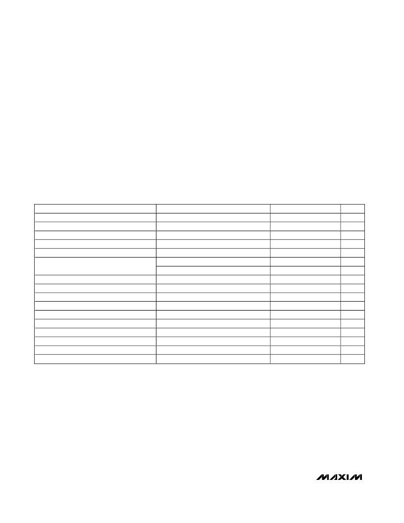
ELECTRICAL CHARACTERISTICS
(V
CC
= +2.97V to +5.5V, PECL outputs terminated with 50
to V
CC
- 2V, R1 = 100k
, T
A
= -40°C to +85°C, unless otherwise noted.
Typical values are at V
CC
= +3.3V, T
A
= +25°C.) (Note 1)
PARAMETER
CONDITIONS
MIN
TYP
22
5
27
MAX
45
8.0
100
-880
-1550
+3.0
+3.6
2.7
UNITS
mA
dB
μA
mV
mV
dB
dB
mV
P-P
mV
P-P
mV
P-P
mV
P-P
V
μA
V
ns
ps
μs
Supply Current
LOS Hysteresis
Squelch Input Current
PECL Output-Voltage High
PECL Output-Voltage Low
PECL outputs open
Input = 4.0mV
P-P
(Note 2)
3.0
(Note 3)
(Note 3)
Input = 7mV
P-P
or 90mV
P-P
, 0
°
C to +85
°
C
Input = 7mV
P-P
or 90mV
P-P
, -40
°
C to +85
°
C
-1085
-1830
-3.0
-3.6
LOS Assert Accuracy
Minimum LOS Assert Input
Maximum LOS Deassert Input
Input Sensitivity
Input Overload
TTL Output High
TTL Output Leakage
TTL Output Low
Data Output Transition Time
Pulse-Width Distortion
LOS, SD Assert/Deassert Time
143
(Note 4)
(Note 4)
R
LOS
= 4.7k
to 10k
(Note 5)
I
OL
= 800μA
20% to 80%, Input > 4mV
P-P
(Note 4)
Input > 4mV
P-P
(Notes 4, 6)
C
FILTER
= 0.01μF
1
4
1500
2.4
3.0
1
0.2
0.8
50
10
20
0.5
1.20
250
0.35
Note 1:
Dice are tested and guaranteed only at T
A
= +25°C.
Note 2:
LOS hysteresis = 20log(V
LOS-DEASSERT
/ V
LOS-ASSERT
).
Note 3:
Relative to supply voltage (V
CCO
).
Note 4:
AC characteristics are guaranteed by design and characterization.
Note 5:
Input < LOS threshold (LOS = HIGH), V
LOS
= 2.4V.
Note 6:
Pulse-width distortion = [(width of wider pulse) - (width of narrower pulse)] / 2, measured with 100Mbps 1-0 pattern.
相關(guān)PDF資料 |
PDF描述 |
|---|---|
| MAX3969E | 2x2 Crosspoint Switch : LVDS Outputs 16-SOIC -40 to 85 |
| MAX397EQI | Precision, 16-Channel/Dual 8-Channel, Low-Voltage, CMOS Analog Multiplexers |
| MAX396CQI | Precision, 16-Channel/Dual 8-Channel, Low-Voltage, CMOS Analog Multiplexers |
| MAX396EQI | Precision, 16-Channel/Dual 8-Channel, Low-Voltage, CMOS Analog Multiplexers |
| MAX397EWI | Precision, 16-Channel/Dual 8-Channel, Low-Voltage, CMOS Analog Multiplexers |
相關(guān)代理商/技術(shù)參數(shù) |
參數(shù)描述 |
|---|---|
| MAX3969E/D | 功能描述:限幅放大器 RoHS:否 制造商:Micrel 輸入電壓范圍(最大值):3.6 V 工作電源電壓:3.3 V 電源電流:40 mA 工作溫度范圍:- 40 C to + 85 C 封裝 / 箱體:MSOP-10 封裝:Tube |
| MAX3969E/D DIE | 制造商:Maxim Integrated Products 功能描述: |
| MAX3969E/D+ | 功能描述:限幅放大器 RoHS:否 制造商:Micrel 輸入電壓范圍(最大值):3.6 V 工作電源電壓:3.3 V 電源電流:40 mA 工作溫度范圍:- 40 C to + 85 C 封裝 / 箱體:MSOP-10 封裝:Tube |
| MAX3969ETP | 功能描述:限幅放大器 270Mbps SFP LED RoHS:否 制造商:Micrel 輸入電壓范圍(最大值):3.6 V 工作電源電壓:3.3 V 電源電流:40 mA 工作溫度范圍:- 40 C to + 85 C 封裝 / 箱體:MSOP-10 封裝:Tube |
| MAX3969ETP+ | 功能描述:限幅放大器 270Mbps SFP LED RoHS:否 制造商:Micrel 輸入電壓范圍(最大值):3.6 V 工作電源電壓:3.3 V 電源電流:40 mA 工作溫度范圍:- 40 C to + 85 C 封裝 / 箱體:MSOP-10 封裝:Tube |
發(fā)布緊急采購(gòu),3分鐘左右您將得到回復(fù)。