- 您現(xiàn)在的位置:買賣IC網(wǎng) > PDF目錄2088 > MAX3658AETA+T (Maxim Integrated Products)IC AMP TRANSIMPEDANCE 8-TDFN PDF資料下載
參數(shù)資料
| 型號: | MAX3658AETA+T |
| 廠商: | Maxim Integrated Products |
| 文件頁數(shù): | 13/15頁 |
| 文件大小: | 0K |
| 描述: | IC AMP TRANSIMPEDANCE 8-TDFN |
| 產(chǎn)品培訓(xùn)模塊: | Lead (SnPb) Finish for COTS Obsolescence Mitigation Program |
| 標(biāo)準(zhǔn)包裝: | 2,500 |
| 類型: | 轉(zhuǎn)阻放大器 |
| 應(yīng)用: | 光纖學(xué)網(wǎng)絡(luò) |
| 安裝類型: | 表面貼裝 |
| 封裝/外殼: | 8-WDFN 裸露焊盤 |
| 供應(yīng)商設(shè)備封裝: | 8-TDFN-EP(3x3) |
| 包裝: | 帶卷 (TR) |
Output Buffer
The output buffer is designed to drive a 150
Ω differen-
tial load between OUT+ and OUT-. For optimum supply
noise rejection, the MAX3658 should be terminated with
a differential load. The MAX3658 single-ended outputs
do not drive a DC-coupled grounded load. The outputs
should be AC-coupled or terminated to VCC. If a single-
ended output is required, both the used and the unused
outputs should be terminated in a similar manner (see
the
Interface Schematics section).
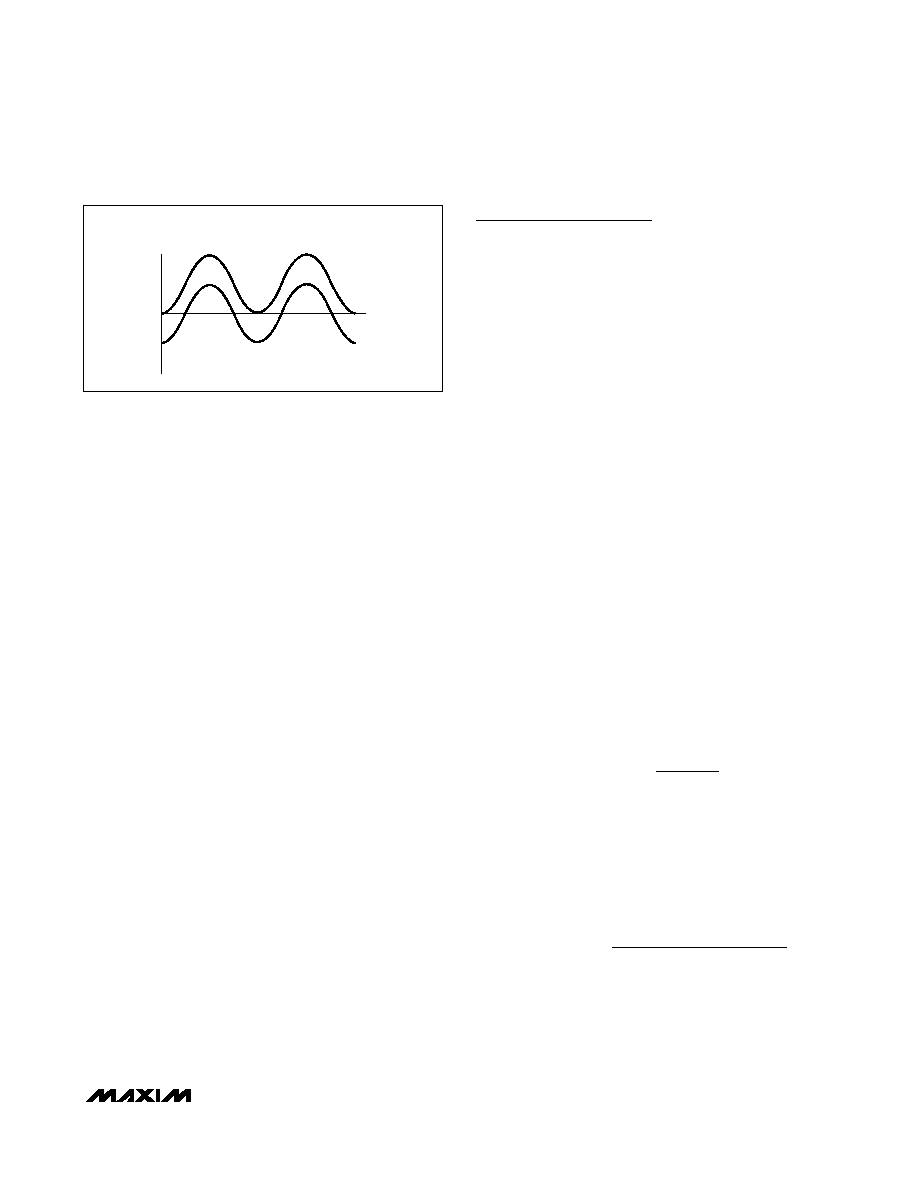
DC Cancellation Circuit
The DC cancellation circuit uses low-frequency feed-
back to remove the DC component of the input signal
(Figure 2). This feature centers the input signal within
the transimpedance amplifier’s linear range, thereby
reducing pulse-width distortion.
The DC cancellation circuit is internally compensated
and does not require external capacitors. This circuit
minimizes pulse-width distortion for data sequences
that exhibit a 50% mark density. A mark density signifi-
cantly different from 50% causes the MAX3658 to gen-
erate pulse-width distortion. Grounding the FILT pin
disables the DC cancellation circuit. For normal opera-
tion, the DC cancellation circuit must be enabled.
The DC cancellation current is drawn from the input and
creates noise. For low-level signals with little or no DC
component, the added noise is insignificant. However,
amplifier noise increases for signals with significant DC
component (see the
Typical Operating Characteristics).
Photocurrent Monitor
The MAX3658 includes an average photocurrent moni-
tor. The current sourced from MON to ground is approxi-
mately equal to the DC current at IN.
Design Procedure
Select Photodiode
Noise performance and bandwidth are adversely affected
by capacitance on the TIA input node. Select a low-
capacitance photodiode to minimize the total input capac-
itance on this pin. The MAX3658 is optimized for 0.5pF of
capacitance on the input. Assembling the MAX3658 in die
form using chip and wire technology provides the lowest
capacitance input and the best possible performance.
Select CFILT
Supply voltage noise at the cathode of the photodiode
produces a current i = CPD dv/dt, which reduces the
receiver sensitivity (CPD is the photodiode capaci-
tance). The filter resistor of the MAX3658 combined
with an external capacitor, can be used to reduce the
effect of supply noise on performance (see the
Typical
Operating Circuit). Current generated by supply noise
voltage is divided between CFILT and CPD. To obtain a
good optical sensitivity select CFILT
≈ 400pF.
Select Supply Filter
Sensitive optical receivers require wide-band power-
supply decoupling. Power-supply bypassing should
provide low impedance between VCC and ground for
frequencies between 10kHz and 700MHz. Isolate the
MAX3658 from noise sources with LC supply filters and
shielding. Place a supply filter (CVCC2) as close to the
MAX3658 as possible.
Select RMON
If photocurrent monitoring is desired, connect a resistor
between MON and ground to monitor the average pho-
tocurrent. Select RMON as large as possible:
where IMONMAX is the largest average input current
observed. An ammeter can also monitor the current out
of the MON pin.
Select Coupling Capacitors
A receiver built with the MAX3658 will have a bandpass
frequency response. The low-frequency cutoff due to
the coupling capacitors and load resistors is:
LFC
RC
TERM
LOAD
COUPLE
=
××
1
2
π
R
V
I
MON
MONMAX
.
=
22
MAX3658
622Mbps, Low-Noise, High-Gain
Transimpedance Preamplifier
_______________________________________________________________________________________
7
AMPLITUDE
INPUT FROM PHOTODIODE
TIME
INPUT AFTER DC CANCELLATION
Figure 2. DC Cancellation Effect on Input
相關(guān)PDF資料 |
PDF描述 |
|---|---|
| MAX3660ETE+T | IC TRANSIMPEDANCE AMP 16TQFN-EP |
| MAX3664ESA+T | IC PREAMP 622MBPS ULP 3.3V 8SOIC |
| MAX3665EUA+T | IC PREAMP 622MBPS TRANS 8-UMAX |
| MAX3679AETJ+T | IC CLOCK GENERATOR LVPECL 32TQFN |
| MAX3747EUB+T | IC AMP LIMITING SFP 10-UMAX |
相關(guān)代理商/技術(shù)參數(shù) |
參數(shù)描述 |
|---|---|
| MAX3658AEVKIT | 制造商:Maxim Integrated Products 功能描述:622MBPS, LOW-NOISE, HIGH-GAIN TRANSIMPEDANCE - Bulk |
| MAX3658BE/D | 功能描述:特殊用途放大器 RoHS:否 制造商:Texas Instruments 通道數(shù)量:Single 共模抑制比(最小值): 輸入補償電壓: 工作電源電壓:3 V to 5.5 V 電源電流:5 mA 最大功率耗散: 最大工作溫度:+ 70 C 最小工作溫度:- 40 C 安裝風(fēng)格:SMD/SMT 封裝 / 箱體:QFN-20 封裝:Reel |
| MAX365C/D | 功能描述:模擬開關(guān) IC RoHS:否 制造商:Texas Instruments 開關(guān)數(shù)量:2 開關(guān)配置:SPDT 開啟電阻(最大值):0.1 Ohms 切換電壓(最大): 開啟時間(最大值): 關(guān)閉時間(最大值): 工作電源電壓:2.7 V to 4.5 V 最大工作溫度:+ 85 C 安裝風(fēng)格:SMD/SMT 封裝 / 箱體:DSBGA-16 |
| MAX365CPE | 功能描述:模擬開關(guān) IC RoHS:否 制造商:Texas Instruments 開關(guān)數(shù)量:2 開關(guān)配置:SPDT 開啟電阻(最大值):0.1 Ohms 切換電壓(最大): 開啟時間(最大值): 關(guān)閉時間(最大值): 工作電源電壓:2.7 V to 4.5 V 最大工作溫度:+ 85 C 安裝風(fēng)格:SMD/SMT 封裝 / 箱體:DSBGA-16 |
| MAX365CPE+ | 功能描述:模擬開關(guān) IC RoHS:否 制造商:Texas Instruments 開關(guān)數(shù)量:2 開關(guān)配置:SPDT 開啟電阻(最大值):0.1 Ohms 切換電壓(最大): 開啟時間(最大值): 關(guān)閉時間(最大值): 工作電源電壓:2.7 V to 4.5 V 最大工作溫度:+ 85 C 安裝風(fēng)格:SMD/SMT 封裝 / 箱體:DSBGA-16 |
發(fā)布緊急采購,3分鐘左右您將得到回復(fù)。