- 您現(xiàn)在的位置:買賣IC網(wǎng) > PDF目錄369889 > M68HC000 (Motorola, Inc.) 16-/32-Bit Microprocessor(16/32位微處理器) PDF資料下載
參數(shù)資料
| 型號: | M68HC000 |
| 廠商: | Motorola, Inc. |
| 英文描述: | 16-/32-Bit Microprocessor(16/32位微處理器) |
| 中文描述: | 16/32位微處理器(16/32位微處理器) |
| 文件頁數(shù): | 157/184頁 |
| 文件大?。?/td> | 1006K |
| 代理商: | M68HC000 |
第1頁第2頁第3頁第4頁第5頁第6頁第7頁第8頁第9頁第10頁第11頁第12頁第13頁第14頁第15頁第16頁第17頁第18頁第19頁第20頁第21頁第22頁第23頁第24頁第25頁第26頁第27頁第28頁第29頁第30頁第31頁第32頁第33頁第34頁第35頁第36頁第37頁第38頁第39頁第40頁第41頁第42頁第43頁第44頁第45頁第46頁第47頁第48頁第49頁第50頁第51頁第52頁第53頁第54頁第55頁第56頁第57頁第58頁第59頁第60頁第61頁第62頁第63頁第64頁第65頁第66頁第67頁第68頁第69頁第70頁第71頁第72頁第73頁第74頁第75頁第76頁第77頁第78頁第79頁第80頁第81頁第82頁第83頁第84頁第85頁第86頁第87頁第88頁第89頁第90頁第91頁第92頁第93頁第94頁第95頁第96頁第97頁第98頁第99頁第100頁第101頁第102頁第103頁第104頁第105頁第106頁第107頁第108頁第109頁第110頁第111頁第112頁第113頁第114頁第115頁第116頁第117頁第118頁第119頁第120頁第121頁第122頁第123頁第124頁第125頁第126頁第127頁第128頁第129頁第130頁第131頁第132頁第133頁第134頁第135頁第136頁第137頁第138頁第139頁第140頁第141頁第142頁第143頁第144頁第145頁第146頁第147頁第148頁第149頁第150頁第151頁第152頁第153頁第154頁第155頁第156頁當(dāng)前第157頁第158頁第159頁第160頁第161頁第162頁第163頁第164頁第165頁第166頁第167頁第168頁第169頁第170頁第171頁第172頁第173頁第174頁第175頁第176頁第177頁第178頁第179頁第180頁第181頁第182頁第183頁第184頁
MOTOROLA
M68000 8-/16-/32-BIT MICROPROCESSORS USER'S MANUAL
10-17
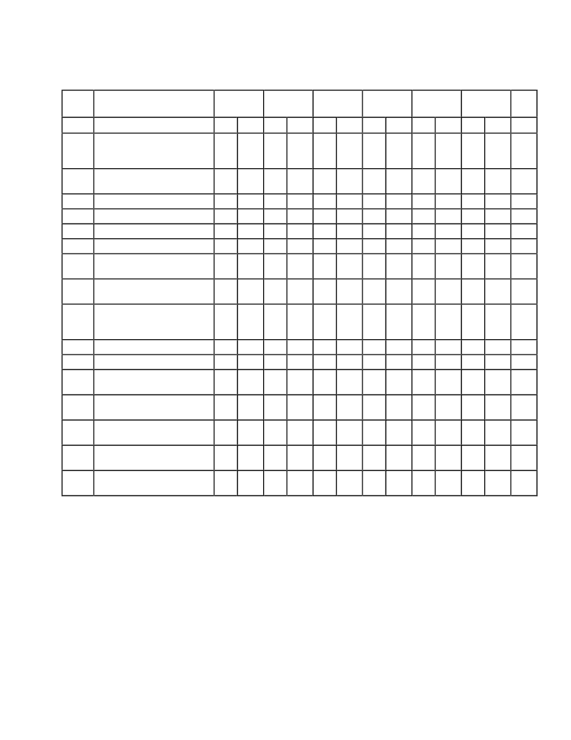
10.12 AC ELECTRICAL SPECIFICATIONS — BUS ARBITRATION
(VCC=5.0
VDC
±
5%; GND=0 VDC, TA=TL TO TH; See Figure s 10-7 – 10-11) (Applies To All Processors
Except The MC68EC000)
Num
Characteristic
8 MHz*
10 MHz*
12.5 MHz*
16.67 MHz
12F
16 MHz
20 MHz
Unit
Min
Max
Min
Max
Min
Max
Min
Max
Min
Max
Min
Max
7
Clock High to Address, Data
Bus High Impedance
(Maximum)
—
80
—
70
—
60
—
50
—
50
—
42
ns
16
Clock High to Control Bus
High Impedance
—
80
—
70
—
60
—
50
—
50
—
42
ns
33
Clock High to
BG
Asserted
—
62
—
50
—
40
0
40
0
30
0
25
ns
34
Clock High to
BG
Negated
—
62
—
50
—
40
0
40
0
30
0
25
ns
35
361
BR
Asserted to
BG
Asserted
1.5
3.5
1.5
3.5
1.5
3.5
1.5
3.5
1.5
3.5
1.5
3.5
Clks
BR
Negated to
BG
Negated
1.5
3.5
1.5
3.5
1.5
3.5
1.5
3.5
1.5
3.5
1.5
3.5
Clks
37
BGACK
Asserted to
BG
Negated
1.5
3.5
1.5
3.5
1.5
3.5
1.5
3.5
1.5
3.5
1.5
3.5
Clks
37A2
BGACK
Asserted to
BR
Negated
20
1.5
Clks
20
1.5
Clks
20
1.5
Clks
10
1.5
Clks
10
1.5
Clks
10
1.5
Clks
Clks/
ns
38
BG
Asserted to Control,
Address, Data Bus High
Impedance (
AS
Negated)
80
70
60
—
50
—
50
—
42
ns
39
BG
Width Negated
1.5
—
1.5
—
1.5
—
1.5
—
1.5
—
1.5
—
Clks
46
BGACK
Width Low
1.5
—
1.5
—
1.5
—
1.5
—
1.5
—
1.5
—
Clks
47
Asynchronous Input Setup
Time
10
—
10
—
10
—
5
—
5
—
5
—
ns
57
BGACK
Negated to
AS, DS
,
R/
W
Driven
1.5
—
1.5
—
1.5
—
1.5
—
1.5
—
1.5
—
Clks
57A
BGACK
Negated to FC,
VMA
Driven
1
—
1
—
1
—
1
—
1
—
1
—
Clks
581
BR
Negated to
AS
,
DS
, R/
W
Driven
1.5
—
1.5
—
1.5
—
1.5
—
1.5
—
1.5
—
Clks
58A1
BR
Negated to FC,
VMA
Driven
1
—
1
—
1
—
1
—
1
—
1
—
Clks
*These specifications represent improvement over previously published specifications for the 8-, 10-, and 12.5-MHz
MC68000 and are valid only for product bearing date codes of 8827 and later.
** Applies only to the MC68HC000 and MC68HC001.
NOTES:
1. Setup time for the synchronous inputs
BGACK
,
IPL0
-
IPL2
, and
VPA
guarantees their recognition at the
next falling edge of the clock.
2.
BR
need fall at this time only in order to insure being recognized at the end of the bus cycle.
3. Timing measurements are referenced to and from a low voltage of 0.8 volt and a high voltage of 2.0 volts,
unless otherwise noted. The voltage swing through this range should start outside and pass through the
range such that the rise or fall will be lienar between 0.8 volt and 2.0 volts.
4. The processor will negate
BG
and begin driving the bus again if external arbitration logic negates
BR
before
asserting
BGACK
.
5. The minimum value must be met to guarantee proper operation. If the maximum value is exceeded,
BG
may
be reasserted.
相關(guān)PDF資料 |
PDF描述 |
|---|---|
| M68HC001 | 16-/32-Bit Microprocessor(16/32位微處理器) |
| M68EC000 | 16/32 Bit Microprocesso(16/32位微處理器) |
| M68HC16 | 16-Bit Microcontroller(16位微控制器) |
| MAC08BT1 | TRIAC 0.8 AMPERE RMS 200 thru 600 Volts |
| MAC08MT1 | SENSITIVE GATE TRIACS |
相關(guān)代理商/技術(shù)參數(shù) |
參數(shù)描述 |
|---|---|
| M68HC05 | 制造商:FREESCALE 制造商全稱:Freescale Semiconductor, Inc 功能描述:Microcontrollers |
| M68HC05_13 | 制造商:FREESCALE 制造商全稱:Freescale Semiconductor, Inc 功能描述:M68HC05 Microcontrollers |
| M68HC05EVS | 制造商:MOTOROLA 制造商全稱:Motorola, Inc 功能描述:Motorola M68HC05 Family Evaluation System |
| M68HC05M68H | 制造商:MOTOROLA 制造商全稱:Motorola, Inc 功能描述:HCMOS Microcontroller Unit |
| M68HC08 | 制造商:FREESCALE 制造商全稱:Freescale Semiconductor, Inc 功能描述:Microcontrollers |
發(fā)布緊急采購,3分鐘左右您將得到回復(fù)。