- 您現(xiàn)在的位置:買(mǎi)賣(mài)IC網(wǎng) > PDF目錄17043 > M52277EVB (Freescale Semiconductor)BOARD DEMO FOR MCF5227 PDF資料下載
參數(shù)資料
| 型號(hào): | M52277EVB |
| 廠商: | Freescale Semiconductor |
| 文件頁(yè)數(shù): | 19/46頁(yè) |
| 文件大小: | 0K |
| 描述: | BOARD DEMO FOR MCF5227 |
| 標(biāo)準(zhǔn)包裝: | 1 |
| 系列: | ColdFire® |
| 類(lèi)型: | MCU |
| 適用于相關(guān)產(chǎn)品: | MCF52277 |
| 所含物品: | 板 |
第1頁(yè)第2頁(yè)第3頁(yè)第4頁(yè)第5頁(yè)第6頁(yè)第7頁(yè)第8頁(yè)第9頁(yè)第10頁(yè)第11頁(yè)第12頁(yè)第13頁(yè)第14頁(yè)第15頁(yè)第16頁(yè)第17頁(yè)第18頁(yè)當(dāng)前第19頁(yè)第20頁(yè)第21頁(yè)第22頁(yè)第23頁(yè)第24頁(yè)第25頁(yè)第26頁(yè)第27頁(yè)第28頁(yè)第29頁(yè)第30頁(yè)第31頁(yè)第32頁(yè)第33頁(yè)第34頁(yè)第35頁(yè)第36頁(yè)第37頁(yè)第38頁(yè)第39頁(yè)第40頁(yè)第41頁(yè)第42頁(yè)第43頁(yè)第44頁(yè)第45頁(yè)第46頁(yè)
MCF5227x ColdFire Microprocessor Data Sheet, Rev. 8
Electrical Characteristics
Freescale Semiconductor
26
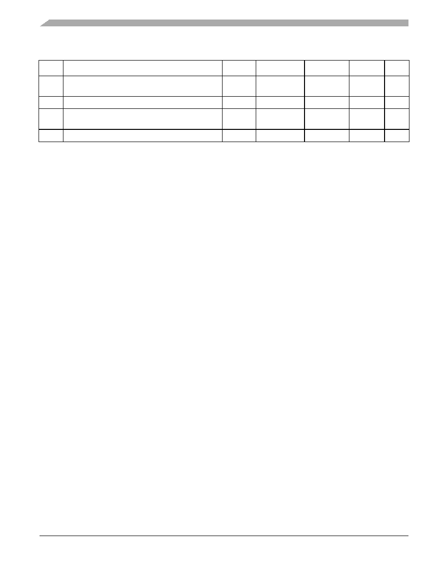
DD8
Data and Data Mask Output Hold (DQS
→DQ) Relative
to DQS (DDR Write Mode)
tDQDMI
1.0
—
ns
7
DD9
Input Data Skew Relative to DQS (Input Setup)
tDVDQ
—1
ns
8
DD10 Input Data Hold Relative to DQS
tDIDQ
0.25
× SD_CLK
+0.5ns
—ns
9
DD11 DQS falling edge from SDCLK rising (output hold time) tDQLSDCH
0.5
—
ns
1 The frequency of operation is either 2x or 4x the FB_CLK frequency of operation. FlexBus and SDRAM clock operate at the
same frequency as the internal bus clock.
2 SD_CLK is one SDRAM clock in ns.
3 Pulse-width high plus pulse-width low cannot exceed minimum or maximum clock period.
4 Command output valid should be one-half the memory bus clock (SD_CLK) plus some minor adjustments for process,
temperature, and voltage variations.
5 This specification relates to the required input setup time of today’s DDR memories. The device’s output setup should be larger
than the input setup of the DDR memories. If it is not larger, then the input setup on the memory will be in violation.
MEM_DATA[31:24] is relative to MEM_DQS[3], MEM_DATA[23:16] is relative to MEM_DQS[2], MEM_DATA[15:8] is relative to
MEM_DQS[1], and MEM_DATA[7:0] is relative MEM_DQS[0].
6 The first data beat will be valid before the first rising edge of DQS and after the DQS write preamble. The remaining data beats
will be valid for each subsequent DQS edge.
7 This specification relates to the required hold time of today’s DDR memories. MEM_DATA[31:24] is relative to MEM_DQS[3],
MEM_DATA[23:16] is relative to MEM_DQS[2], MEM_DATA[15:8] is relative to MEM_DQS[1], and MEM_DATA[7:0] is relative
MEM_DQS[0].
8 Data input skew is derived from each DQS clock edge. It begins with a DQS transition and ends when the last data line
becomes valid. This input skew must include DDR memory output skew and system-level board skew (due to routing or other
factors).
9 Data input hold is derived from each DQS clock edge. It begins with a DQS transition and ends when the first data line becomes
invalid.
Table 15. DDR Timing Specifications (continued)
Num
Characteristic
Symbol
Min
Max
Unit
Notes
相關(guān)PDF資料 |
PDF描述 |
|---|---|
| 0210490925 | CABLE JUMPER 1.25MM .076M 23POS |
| ECM12DSEH-S13 | CONN EDGECARD 24POS .156 EXTEND |
| VI-J1R-EY | CONVERTER MINIMOD DC/DC 7.5V 50W |
| VE-21T-EY | CONVERTER MOD DC/DC 6.5V 50W |
| 0210490924 | CABLE JUMPER 1.25MM .076M 23POS |
相關(guān)代理商/技術(shù)參數(shù) |
參數(shù)描述 |
|---|---|
| M5228FP | 制造商:Panasonic Industrial Company 功能描述:IC |
| M5228P | 制造商:Panasonic Industrial Company 功能描述:IC |
| M5229 | 制造商:Panasonic Industrial Company 功能描述:DISCD IC |
| M-522CT | 制造商:NEC 制造商全稱:NEC 功能描述:DC Line Fileters |
| M522D | 制造商:GOSSEN METRAWATT 功能描述:PSI MODULE PROFITEST PSI-BC |
發(fā)布緊急采購(gòu),3分鐘左右您將得到回復(fù)。