- 您現(xiàn)在的位置:買賣IC網(wǎng) > PDF目錄45050 > M44C090-XXX-FL16 (TEMIC SEMICONDUCTORS) 8-BIT, MROM, 16 MHz, MICROCONTROLLER, PDSO16 PDF資料下載
參數(shù)資料
| 型號(hào): | M44C090-XXX-FL16 |
| 廠商: | TEMIC SEMICONDUCTORS |
| 元件分類: | 微控制器/微處理器 |
| 英文描述: | 8-BIT, MROM, 16 MHz, MICROCONTROLLER, PDSO16 |
| 文件頁(yè)數(shù): | 227/319頁(yè) |
| 文件大小: | 11009K |
| 代理商: | M44C090-XXX-FL16 |
第1頁(yè)第2頁(yè)第3頁(yè)第4頁(yè)第5頁(yè)第6頁(yè)第7頁(yè)第8頁(yè)第9頁(yè)第10頁(yè)第11頁(yè)第12頁(yè)第13頁(yè)第14頁(yè)第15頁(yè)第16頁(yè)第17頁(yè)第18頁(yè)第19頁(yè)第20頁(yè)第21頁(yè)第22頁(yè)第23頁(yè)第24頁(yè)第25頁(yè)第26頁(yè)第27頁(yè)第28頁(yè)第29頁(yè)第30頁(yè)第31頁(yè)第32頁(yè)第33頁(yè)第34頁(yè)第35頁(yè)第36頁(yè)第37頁(yè)第38頁(yè)第39頁(yè)第40頁(yè)第41頁(yè)第42頁(yè)第43頁(yè)第44頁(yè)第45頁(yè)第46頁(yè)第47頁(yè)第48頁(yè)第49頁(yè)第50頁(yè)第51頁(yè)第52頁(yè)第53頁(yè)第54頁(yè)第55頁(yè)第56頁(yè)第57頁(yè)第58頁(yè)第59頁(yè)第60頁(yè)第61頁(yè)第62頁(yè)第63頁(yè)第64頁(yè)第65頁(yè)第66頁(yè)第67頁(yè)第68頁(yè)第69頁(yè)第70頁(yè)第71頁(yè)第72頁(yè)第73頁(yè)第74頁(yè)第75頁(yè)第76頁(yè)第77頁(yè)第78頁(yè)第79頁(yè)第80頁(yè)第81頁(yè)第82頁(yè)第83頁(yè)第84頁(yè)第85頁(yè)第86頁(yè)第87頁(yè)第88頁(yè)第89頁(yè)第90頁(yè)第91頁(yè)第92頁(yè)第93頁(yè)第94頁(yè)第95頁(yè)第96頁(yè)第97頁(yè)第98頁(yè)第99頁(yè)第100頁(yè)第101頁(yè)第102頁(yè)第103頁(yè)第104頁(yè)第105頁(yè)第106頁(yè)第107頁(yè)第108頁(yè)第109頁(yè)第110頁(yè)第111頁(yè)第112頁(yè)第113頁(yè)第114頁(yè)第115頁(yè)第116頁(yè)第117頁(yè)第118頁(yè)第119頁(yè)第120頁(yè)第121頁(yè)第122頁(yè)第123頁(yè)第124頁(yè)第125頁(yè)第126頁(yè)第127頁(yè)第128頁(yè)第129頁(yè)第130頁(yè)第131頁(yè)第132頁(yè)第133頁(yè)第134頁(yè)第135頁(yè)第136頁(yè)第137頁(yè)第138頁(yè)第139頁(yè)第140頁(yè)第141頁(yè)第142頁(yè)第143頁(yè)第144頁(yè)第145頁(yè)第146頁(yè)第147頁(yè)第148頁(yè)第149頁(yè)第150頁(yè)第151頁(yè)第152頁(yè)第153頁(yè)第154頁(yè)第155頁(yè)第156頁(yè)第157頁(yè)第158頁(yè)第159頁(yè)第160頁(yè)第161頁(yè)第162頁(yè)第163頁(yè)第164頁(yè)第165頁(yè)第166頁(yè)第167頁(yè)第168頁(yè)第169頁(yè)第170頁(yè)第171頁(yè)第172頁(yè)第173頁(yè)第174頁(yè)第175頁(yè)第176頁(yè)第177頁(yè)第178頁(yè)第179頁(yè)第180頁(yè)第181頁(yè)第182頁(yè)第183頁(yè)第184頁(yè)第185頁(yè)第186頁(yè)第187頁(yè)第188頁(yè)第189頁(yè)第190頁(yè)第191頁(yè)第192頁(yè)第193頁(yè)第194頁(yè)第195頁(yè)第196頁(yè)第197頁(yè)第198頁(yè)第199頁(yè)第200頁(yè)第201頁(yè)第202頁(yè)第203頁(yè)第204頁(yè)第205頁(yè)第206頁(yè)第207頁(yè)第208頁(yè)第209頁(yè)第210頁(yè)第211頁(yè)第212頁(yè)第213頁(yè)第214頁(yè)第215頁(yè)第216頁(yè)第217頁(yè)第218頁(yè)第219頁(yè)第220頁(yè)第221頁(yè)第222頁(yè)第223頁(yè)第224頁(yè)第225頁(yè)第226頁(yè)當(dāng)前第227頁(yè)第228頁(yè)第229頁(yè)第230頁(yè)第231頁(yè)第232頁(yè)第233頁(yè)第234頁(yè)第235頁(yè)第236頁(yè)第237頁(yè)第238頁(yè)第239頁(yè)第240頁(yè)第241頁(yè)第242頁(yè)第243頁(yè)第244頁(yè)第245頁(yè)第246頁(yè)第247頁(yè)第248頁(yè)第249頁(yè)第250頁(yè)第251頁(yè)第252頁(yè)第253頁(yè)第254頁(yè)第255頁(yè)第256頁(yè)第257頁(yè)第258頁(yè)第259頁(yè)第260頁(yè)第261頁(yè)第262頁(yè)第263頁(yè)第264頁(yè)第265頁(yè)第266頁(yè)第267頁(yè)第268頁(yè)第269頁(yè)第270頁(yè)第271頁(yè)第272頁(yè)第273頁(yè)第274頁(yè)第275頁(yè)第276頁(yè)第277頁(yè)第278頁(yè)第279頁(yè)第280頁(yè)第281頁(yè)第282頁(yè)第283頁(yè)第284頁(yè)第285頁(yè)第286頁(yè)第287頁(yè)第288頁(yè)第289頁(yè)第290頁(yè)第291頁(yè)第292頁(yè)第293頁(yè)第294頁(yè)第295頁(yè)第296頁(yè)第297頁(yè)第298頁(yè)第299頁(yè)第300頁(yè)第301頁(yè)第302頁(yè)第303頁(yè)第304頁(yè)第305頁(yè)第306頁(yè)第307頁(yè)第308頁(yè)第309頁(yè)第310頁(yè)第311頁(yè)第312頁(yè)第313頁(yè)第314頁(yè)第315頁(yè)第316頁(yè)第317頁(yè)第318頁(yè)第319頁(yè)
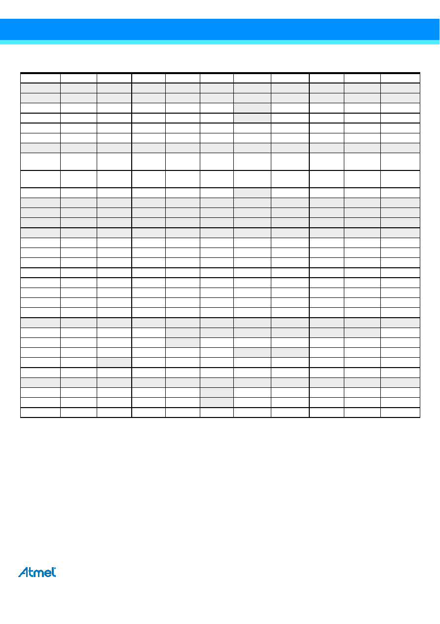
302
Atmel ATmega16/32/64/M1/C1 [DATASHEET]
7647K–AVR–12/13
(0x99)
Reserved
–
(0x98)
Reserved
–
(0x97)
AC3CON
AC3EN
AC3IE
AC3IS1
AC3IS0
–
AC3M2
AC3M1
AC3M0
(0x96)
AC2CON
AC2EN
AC2IE
AC2IS1
AC2IS0
–
AC2M2
AC2M1
AC2M0
(0x95)
AC1CON
AC1EN
AC1IE
AC1IS1
AC1IS0
AC1ICE
AC1M2
AC1M1
AC1M0
(0x94)
AC0CON
AC0EN
AC0IE
AC0IS1
AC0IS0
ACCKSEL
AC0M2
AC0M1
AC0M0
(0x93)
Reserved
–
(0x92)
DACH
- / DAC9
- / DAC8
- / DAC7
- / DAC6
- / DAC5
- / DAC4
DAC9 /
DAC3
DAC8 /
DAC2
(0x91)
DACL
DAC7 /
DAC1
DAC6
/DAC0
DAC5 / -
DAC4 / -
DAC3 / -
DAC2 / -
DAC1 / -
DAC0 /
(0x90)
DACON
DAATE
DATS2
DATS1
DATS0
–
DALA
DAOE
DAEN
(0x8F)
Reserved
–
(0x8E)
Reserved
–
(0x8D)
Reserved
–
(0x8C)
Reserved
–
(0x8B)
OCR1BH
OCR1B15
OCR1B14
OCR1B13
OCR1B12
OCR1B11
OCR1B10
OCR1B9
OCR1B8
(0x8A)
OCR1BL
OCR1B7
OCR1B6
OCR1B5
OCR1B4
OCR1B3
OCR1B2
OCR1B1
OCR1B0
(0x89)
OCR1AH
OCR1A15
OCR1A14
OCR1A13
OCR1A12
OCR1A11
OCR1A10
OCR1A9
OCR1A8
(0x88)
OCR1AL
OCR1A7
OCR1A6
OCR1A5
OCR1A4
OCR1A3
OCR1A2
OCR1A1
OCR1A0
(0x87)
ICR1H
ICR115
ICR114
ICR113
ICR112
ICR111
ICR110
ICR19
ICR18
(0x86)
ICR1L
ICR17
ICR16
ICR15
ICR14
ICR13
ICR12
ICR11
ICR10
(0x85)
TCNT1H
TCNT115
TCNT114
TCNT113
TCNT112
TCNT111
TCNT110
TCNT19
TCNT18
(0x84)
TCNT1L
TCNT17
TCNT16
TCNT15
TCNT14
TCNT13
TCNT12
TCNT11
TCNT10
(0x83)
Reserved
–
(0x82)
TCCR1C
FOC1A
FOC1B
–
(0x81)
TCCR1B
ICNC1
ICES1
–
WGM13
WGM12
CS12
CS11
CS10
(0x80)
TCCR1A
COM1A1
COM1A0
COM1B1
COM1B0
–
–WGM11
WGM10
(0x7F)
DIDR1
–
AMP2PD
ACMP0D
AMP0PD
AMP0ND
ADC10D
ADC9D
ADC8D
(0x7E)
DIDR0
ADC7D
ADC6D
ADC5D
ADC4D
ADC3D
ADC2D
ADC1D
ADC0D
(0x7D)
Reserved
–
(0x7C)
ADMUX
REFS1
REFS0
ADLAR
–
MUX3
MUX2
MUX1
MUX0
(0x7B)
ADCSRB
ADHSM
ISRCEN
AREFEN
–
ADTS3
ADTS2
ADTS1
ADTS0
(0x7A)
ADCSRA
ADEN
ADSC
ADATE
ADIF
ADIE
ADPS2
ADPS1
ADPS0
29.
Register Summary (Continued)
Address
Name
Bit 7
Bit 6
Bit 5
Bit 4
Bit 3
Bit 2
Bit 1
Bit 0
Page
Notes: 1. For compatibility with future devices, reserved bits should be written to zero if accessed. Reserved I/O memory addresses
should never be written.
2. I/O registers within the address range 0x00 - 0x1F are directly bit-accessible using the SBI and CBI instructions. In these
registers, the value of single bits can be checked by using the SBIS and SBIC instructions.
3. Some of the status flags are cleared by writing a logical one to them. Note that, unlike most other AVRs, the CBI and SBI
instructions will only operate on the specified bit, and can therefore be used on registers containing such status flags. The
CBI and SBI instructions work with registers 0x00 to 0x1F only.
4. When using the I/O specific commands IN and OUT, the I/O addresses 0x00 - 0x3F must be used. When addressing I/O
Registers as data space using LD and ST instructions, 0x20 must be added to these addresses. The
ATmega16/32/64/M1/C1 is a complex microcontroller with more peripheral units than can be supported within the 64 loca-
tion reserved in Opcode for the IN and OUT instructions. For the Extended I/O space from 0x60 - 0xFF in SRAM, only the
ST/STS/STD and LD/LDS/LDD instructions can be used.
5. These registers are only available on ATmega32/64M1. For other products described in this datasheet, these locations are
reserved.
相關(guān)PDF資料 |
PDF描述 |
|---|---|
| M44C090-XXX-DIT | 4-BIT, MROM, 4 MHz, MICROCONTROLLER, UUC |
| M48ST59W-70MH1TR | 0 TIMER(S), REAL TIME CLOCK, PDSO44 |
| M48ST59W-100MH1 | 0 TIMER(S), REAL TIME CLOCK, PDSO44 |
| M48T02-150PC1 | 0 TIMER(S), REAL TIME CLOCK, PDIP24 |
| M48T18-100MH1TR | 0 TIMER(S), REAL TIME CLOCK, PDSO28 |
相關(guān)代理商/技術(shù)參數(shù) |
參數(shù)描述 |
|---|---|
| M44C890 | 制造商:ATMEL 制造商全稱:ATMEL Corporation 功能描述:Low-Current Microcontroller for Wireless Communication |
| M44C890-H | 制造商:ATMEL 制造商全稱:ATMEL Corporation 功能描述:Low-Current Microcontroller for Wireless Communication |
| M44S05K4F1 | 功能描述:汽車連接器 MX44 Terminals RoHS:否 制造商:Amphenol SINE Systems 產(chǎn)品:Contacts 系列:ATP 位置數(shù)量: 型式:Female 安裝風(fēng)格: 端接類型: 觸點(diǎn)電鍍:Nickel |
| M44T332538880MHZ | 制造商:MEC 功能描述: |
| M44T3338880MHZ | 制造商:MEC 功能描述: |
發(fā)布緊急采購(gòu),3分鐘左右您將得到回復(fù)。