- 您現(xiàn)在的位置:買賣IC網(wǎng) > PDF目錄45046 > M38507M8-XXXSP 8-BIT, MROM, 8 MHz, MICROCONTROLLER, PDIP42 PDF資料下載
參數(shù)資料
| 型號(hào): | M38507M8-XXXSP |
| 元件分類: | 微控制器/微處理器 |
| 英文描述: | 8-BIT, MROM, 8 MHz, MICROCONTROLLER, PDIP42 |
| 封裝: | 0.600 INCH, 1.78 MM PITCH, PLASTIC, SDIP-42 |
| 文件頁數(shù): | 273/287頁 |
| 文件大小: | 2969K |
| 代理商: | M38507M8-XXXSP |
第1頁第2頁第3頁第4頁第5頁第6頁第7頁第8頁第9頁第10頁第11頁第12頁第13頁第14頁第15頁第16頁第17頁第18頁第19頁第20頁第21頁第22頁第23頁第24頁第25頁第26頁第27頁第28頁第29頁第30頁第31頁第32頁第33頁第34頁第35頁第36頁第37頁第38頁第39頁第40頁第41頁第42頁第43頁第44頁第45頁第46頁第47頁第48頁第49頁第50頁第51頁第52頁第53頁第54頁第55頁第56頁第57頁第58頁第59頁第60頁第61頁第62頁第63頁第64頁第65頁第66頁第67頁第68頁第69頁第70頁第71頁第72頁第73頁第74頁第75頁第76頁第77頁第78頁第79頁第80頁第81頁第82頁第83頁第84頁第85頁第86頁第87頁第88頁第89頁第90頁第91頁第92頁第93頁第94頁第95頁第96頁第97頁第98頁第99頁第100頁第101頁第102頁第103頁第104頁第105頁第106頁第107頁第108頁第109頁第110頁第111頁第112頁第113頁第114頁第115頁第116頁第117頁第118頁第119頁第120頁第121頁第122頁第123頁第124頁第125頁第126頁第127頁第128頁第129頁第130頁第131頁第132頁第133頁第134頁第135頁第136頁第137頁第138頁第139頁第140頁第141頁第142頁第143頁第144頁第145頁第146頁第147頁第148頁第149頁第150頁第151頁第152頁第153頁第154頁第155頁第156頁第157頁第158頁第159頁第160頁第161頁第162頁第163頁第164頁第165頁第166頁第167頁第168頁第169頁第170頁第171頁第172頁第173頁第174頁第175頁第176頁第177頁第178頁第179頁第180頁第181頁第182頁第183頁第184頁第185頁第186頁第187頁第188頁第189頁第190頁第191頁第192頁第193頁第194頁第195頁第196頁第197頁第198頁第199頁第200頁第201頁第202頁第203頁第204頁第205頁第206頁第207頁第208頁第209頁第210頁第211頁第212頁第213頁第214頁第215頁第216頁第217頁第218頁第219頁第220頁第221頁第222頁第223頁第224頁第225頁第226頁第227頁第228頁第229頁第230頁第231頁第232頁第233頁第234頁第235頁第236頁第237頁第238頁第239頁第240頁第241頁第242頁第243頁第244頁第245頁第246頁第247頁第248頁第249頁第250頁第251頁第252頁第253頁第254頁第255頁第256頁第257頁第258頁第259頁第260頁第261頁第262頁第263頁第264頁第265頁第266頁第267頁第268頁第269頁第270頁第271頁第272頁當(dāng)前第273頁第274頁第275頁第276頁第277頁第278頁第279頁第280頁第281頁第282頁第283頁第284頁第285頁第286頁第287頁
HARDWARE
3850 Group (Spec. H) User’s Manual
FUNCTIONAL DESCRIPTION
1-68
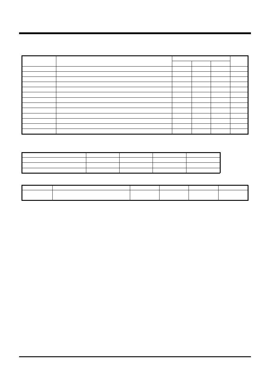
Limits
Parameter
200
100
25
100
25
0
100
50
10
Symbol
Unit
Write cycle time
Address set up time
Address hold time
Data set up time
Data hold time
______
WE set up time
______
WE hold time
_____
CE pulse width
_____
“H” CE pulse width
Program time
Erase all blocks time
_____
RY/BY delay time
_____
RP recovery time
tWC
tAS
tAH
tDS
tDH
tWS
tWH
tCEP
tCEPH
tDAP
tDAE
tEHRL
tPS
Min.
Typ.
Max.
25
1.5
200
ns
s
ns
s
_____
Table 24 Read / Write mode (CE control)
Parameter
Erase all blocks time
Block erase time
Program time (1byte)
1.5
1.0
25
s
Min.
Typ.
Max.
Unit
Table 25 Erase and program operation
Symbol
Min.
Typ.
Max.
Unit
Table 26 VCC power up / power down timing
Parameter
_____
RP = VIH set up time
(after rised VCC = VCC min.)
tVCS
10
Note : The read timing parameter in the command write operation mode is same as that of the read-only mode.
Typical value is at VCC = 5.0 V, Ta = 25 °C condition.
Note : Miserase or miswrite may happen, in case of noise pulse due to the power supply on or off is input to the control pins. Therefore disableing the
write mode is need for prevent from memory data break at the power supply on or off. 10
s (min.) waiting time is need to initiate read or write op-
_____
eration after VCC rises to VCC min. at power supply on. The memory data is protected owing to keep the RP pin VIL level at power supply off. The
_____
RP pin must be kept VIL level for 10
s (min.) after VCC rises to VCC min. at the power supply on. The RP pin must be kept VIL level until the VCC
_____
falls to the GND level at power supply off. RP pin doesn't have latch mode, so RP pin must be kept VIH level during read, erase and program op-
eration.
Flash memory mode Electrical characteristics
(Ta = 25oC, VCC = 4.5 to 5.5V unless otherwise noted)
s
相關(guān)PDF資料 |
PDF描述 |
|---|---|
| M38507F8SP | 8-BIT, MROM, 8 MHz, MICROCONTROLLER, PDIP42 |
| M38503M2H-XXXFP | 8-BIT, MROM, 8 MHz, MICROCONTROLLER, PDSO42 |
| M38507F8FP | 8-BIT, MROM, 8 MHz, MICROCONTROLLER, PDSO42 |
| M38507M8-XXXSP | 8-BIT, MROM, 8 MHz, MICROCONTROLLER, PDIP42 |
| M38504E6FP | 8-BIT, OTPROM, 8 MHz, MICROCONTROLLER, PDSO42 |
相關(guān)代理商/技術(shù)參數(shù) |
參數(shù)描述 |
|---|---|
| M3851 BK001 | 制造商:Alpha Wire Company 功能描述:CBL 7COND 14AWG BLK 1000' |
| M3851 BK002 | 制造商:Alpha Wire Company 功能描述:CBL 7COND 14AWG BLK 500' |
| M3851 BK005 | 制造商:Alpha Wire Company 功能描述:CBL 7COND 14AWG BLK 100' |
| M38510/00102BCB | 制造商:n/a 功能描述:38510/00102 S6I6B 制造商: 功能描述: 制造商:undefined 功能描述: |
| M38510/00103BCA | 制造商:QP Semiconductor 功能描述:NAND GATE, TRIPLE 3-INPUT |
發(fā)布緊急采購,3分鐘左右您將得到回復(fù)。