- 您現(xiàn)在的位置:買賣IC網(wǎng) > PDF目錄370849 > M37754M8C-XXXGP (Mitsubishi Electric Corporation) SINGLE-CHIP 16BIT CMOS MICROCOMPUTER PDF資料下載
參數(shù)資料
| 型號: | M37754M8C-XXXGP |
| 廠商: | Mitsubishi Electric Corporation |
| 英文描述: | SINGLE-CHIP 16BIT CMOS MICROCOMPUTER |
| 中文描述: | 單芯片16位微機的CMOS |
| 文件頁數(shù): | 5/114頁 |
| 文件大小: | 1116K |
| 代理商: | M37754M8C-XXXGP |
第1頁第2頁第3頁第4頁當(dāng)前第5頁第6頁第7頁第8頁第9頁第10頁第11頁第12頁第13頁第14頁第15頁第16頁第17頁第18頁第19頁第20頁第21頁第22頁第23頁第24頁第25頁第26頁第27頁第28頁第29頁第30頁第31頁第32頁第33頁第34頁第35頁第36頁第37頁第38頁第39頁第40頁第41頁第42頁第43頁第44頁第45頁第46頁第47頁第48頁第49頁第50頁第51頁第52頁第53頁第54頁第55頁第56頁第57頁第58頁第59頁第60頁第61頁第62頁第63頁第64頁第65頁第66頁第67頁第68頁第69頁第70頁第71頁第72頁第73頁第74頁第75頁第76頁第77頁第78頁第79頁第80頁第81頁第82頁第83頁第84頁第85頁第86頁第87頁第88頁第89頁第90頁第91頁第92頁第93頁第94頁第95頁第96頁第97頁第98頁第99頁第100頁第101頁第102頁第103頁第104頁第105頁第106頁第107頁第108頁第109頁第110頁第111頁第112頁第113頁第114頁
5
MITSUBISHI MICROCOMPUTERS
M37754M8C-XXXGP, M37754M8C-XXXHP
M37754S4CGP, M37754S4CHP
PRELIMINARY
Notice: This is not a final specification.
Some parametric limits are subject to change.
SINGLE-CHIP 16-BIT CMOS MICROCOMPUTER
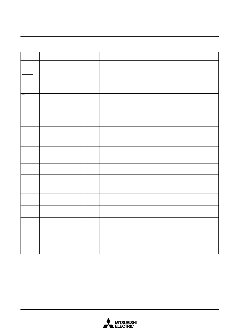
PIN DESCRIPTION (MICROCOMPUTER MODE)
Functions
Input
Input
Input
Output
Output
Input
Input
I/O
I/O
I/O
I/O
I/O
I/O
I/O
I/O
I/O
I/O
Input/
Output
Name
Pin
V
CC
, V
SS
CNV
SS
RESET
X
IN
X
OUT
E
BYTE
(Note)
AV
CC
,
AV
SS
V
REF
P0
0
– P0
7
P1
0
– P1
7
P2
0
– P2
3
,
P2
7
P3
0
– P3
3
P4
0
– P4
7
P5
0
– P5
7
P6
0
– P6
7
P7
0
– P7
7
P8
0
– P8
7
P9
0
– P9
5
Supply 5 V±10 % to V
CC
and 0 V to V
SS
.
This pin controls the processor mode. Connect to V
SS
for single-chip mode or memory
expansion mode. Connect to V
CC
for microprocessor mode and external ROM version.
This is reset input pin. The microcomputer is reset when supplying “L” level to this
pin.
These are I/O pins of internal clock generating circuit. Connect a ceramic or quartz-
crystal resonator between X
IN
and X
OUT
. When an external clock is used, the clock
source should be connected to the X
IN
pin and the X
OUT
pin should be left open.
This pin outputs enable signal E, which indicates access state of data bus for
single-chip mode.
This pin outputs RD signal for memory expansion mode or microprocessor mode.
This pin determines whether the external data bus is 8-bit width or 16-bit width for
memory expansion mode or microprocessor mode. The width is 16 bits when “L”
signal inputs and 8 bits when “H” signal inputs.
Power supply for the A-D converter and the D-A converter. Connect AV
CC
to V
CC
and AV
SS
to V
SS
externally.
This is reference voltage input pin for the A-D converter and the D-A converter.
In single-chip mode, port P0 is an 8-bit I/O port. This port has an I/O direction
register and each pin can be programmed for input or output. These ports are in
the input mode when reset. Address (A
0
- A
7
) is output in memory expansion mode
or microprocessor mode.
In single-chip mode, these pins have the same functions as port P0. Address (A
8
-
A
15
) is output in memory expansion mode or microprocessor mode.
In single-chip mode, these pins have the same functions as port P0. Address (A
16
-
A
19
, A
23
) is output in memory expansion mode or microprocessor mode.
In single-chip mode, these pins have the same functions as port P0. In memory
expansion mode or microprocessor mode, WR, BHE , ALE, and HLDA signals are
output.
In single-chip mode, these pins have the same functions as port P0. In memory
0
, P4
1
, and P4
2
become HOLD and
____
φ
1
output pin respectively. Functions of other pins are
the same as in single-chip mode. In memory expansion mode, P4
2
can be
programmed as I/O port.
In addition to having the same functions as port P0 in single-chip mode, these pins
also function as I/O pins for timer A0, timer A1, timer A2, timer A3, output pins for
motor drive waveform, and input pins for key input interrupt.
In addition to having the same functions as port P0 in single-chip mode, these pins
0
,
____
1
, and INT
2
, and input pins for timer B0, timer B1, and timer B2.
In addition to having the same functions as port P0 in single-chip mode, these pins
also function as input pins for A-D converter.
In addition to having the same functions as port P0 in single-chip mode, these pins
also function as I/O pins for UART0, UART1, output pins for D-A converter, and
input pin for INT
4
.
In addition to having the same functions as port P0 in single-chip mode, these pins
also function as input pin for INT
3
, output pins for motor drive waveform.
In memory expansion mode and microprocessor mode, these pins can be
programmed as address (A
20
- A
22
) or output pins for CS
0
– CS
4
Power supply
CNV
SS
input
Reset input
Clock input
Clock output
Enable output
Bus width select input
Analog supply input
Reference voltage input
I/O port P0
I/O port P1
I/O port P2
I/O port P3
I/O port P4
I/O port P5
I/O port P6
I/O port P7
I/O port P8
I/O port P9
Note:
It is impossible to change the input level of the BYTE pin in each bus cycle. In other words, bus width cannot be switched dynamically. Fix the input
level of the BYTE pin to “H” or “L” according to the bus width used.
相關(guān)PDF資料 |
PDF描述 |
|---|---|
| M37754M8C-XXXHP | SINGLE-CHIP 16BIT CMOS MICROCOMPUTER |
| M37754S4CGP | SINGLE-CHIP 16BIT CMOS MICROCOMPUTER |
| M37754S4CHP | SINGLE-CHIP 16BIT CMOS MICROCOMPUTER |
| M37754 | SINGLE-CHIP 16BIT CMOS MICROCOMPUTER |
| M37754M8C | Single Chip 16 Bits CMOS Microcomputer(16位單片機) |
相關(guān)代理商/技術(shù)參數(shù) |
參數(shù)描述 |
|---|---|
| M37754M8C-XXXHP | 制造商:MITSUBISHI 制造商全稱:Mitsubishi Electric Semiconductor 功能描述:SINGLE-CHIP 16BIT CMOS MICROCOMPUTER |
| M37754S4CGP | 制造商:MITSUBISHI 制造商全稱:Mitsubishi Electric Semiconductor 功能描述:SINGLE-CHIP 16BIT CMOS MICROCOMPUTER |
| M37754S4CHP | 制造商:RENESAS 制造商全稱:Renesas Technology Corp 功能描述:SINGLE-CHIP 16-BIT CMOS MICROCOMPUTER |
| M3775PR-H400CL | 制造商:Bonitron 功能描述:OVERVOLTAGE BRAKING RESISTOR |
| M3775RK-0.75A | 制造商:Bonitron 功能描述:OVERVOLTAGE BRAKING RESISTOR |
發(fā)布緊急采購,3分鐘左右您將得到回復(fù)。