- 您現(xiàn)在的位置:買賣IC網(wǎng) > PDF目錄45034 > M37531E8FP 8-BIT, OTPROM, 8 MHz, MICROCONTROLLER, PDSO36 PDF資料下載
參數(shù)資料
| 型號: | M37531E8FP |
| 元件分類: | 微控制器/微處理器 |
| 英文描述: | 8-BIT, OTPROM, 8 MHz, MICROCONTROLLER, PDSO36 |
| 封裝: | 0.450 INCH, PLASTIC, SSOP-36 |
| 文件頁數(shù): | 86/215頁 |
| 文件大小: | 1365K |
| 代理商: | M37531E8FP |
第1頁第2頁第3頁第4頁第5頁第6頁第7頁第8頁第9頁第10頁第11頁第12頁第13頁第14頁第15頁第16頁第17頁第18頁第19頁第20頁第21頁第22頁第23頁第24頁第25頁第26頁第27頁第28頁第29頁第30頁第31頁第32頁第33頁第34頁第35頁第36頁第37頁第38頁第39頁第40頁第41頁第42頁第43頁第44頁第45頁第46頁第47頁第48頁第49頁第50頁第51頁第52頁第53頁第54頁第55頁第56頁第57頁第58頁第59頁第60頁第61頁第62頁第63頁第64頁第65頁第66頁第67頁第68頁第69頁第70頁第71頁第72頁第73頁第74頁第75頁第76頁第77頁第78頁第79頁第80頁第81頁第82頁第83頁第84頁第85頁當前第86頁第87頁第88頁第89頁第90頁第91頁第92頁第93頁第94頁第95頁第96頁第97頁第98頁第99頁第100頁第101頁第102頁第103頁第104頁第105頁第106頁第107頁第108頁第109頁第110頁第111頁第112頁第113頁第114頁第115頁第116頁第117頁第118頁第119頁第120頁第121頁第122頁第123頁第124頁第125頁第126頁第127頁第128頁第129頁第130頁第131頁第132頁第133頁第134頁第135頁第136頁第137頁第138頁第139頁第140頁第141頁第142頁第143頁第144頁第145頁第146頁第147頁第148頁第149頁第150頁第151頁第152頁第153頁第154頁第155頁第156頁第157頁第158頁第159頁第160頁第161頁第162頁第163頁第164頁第165頁第166頁第167頁第168頁第169頁第170頁第171頁第172頁第173頁第174頁第175頁第176頁第177頁第178頁第179頁第180頁第181頁第182頁第183頁第184頁第185頁第186頁第187頁第188頁第189頁第190頁第191頁第192頁第193頁第194頁第195頁第196頁第197頁第198頁第199頁第200頁第201頁第202頁第203頁第204頁第205頁第206頁第207頁第208頁第209頁第210頁第211頁第212頁第213頁第214頁第215頁
7531 Group User’s Manual
3-60
APPENDIX
3.5 List of registers
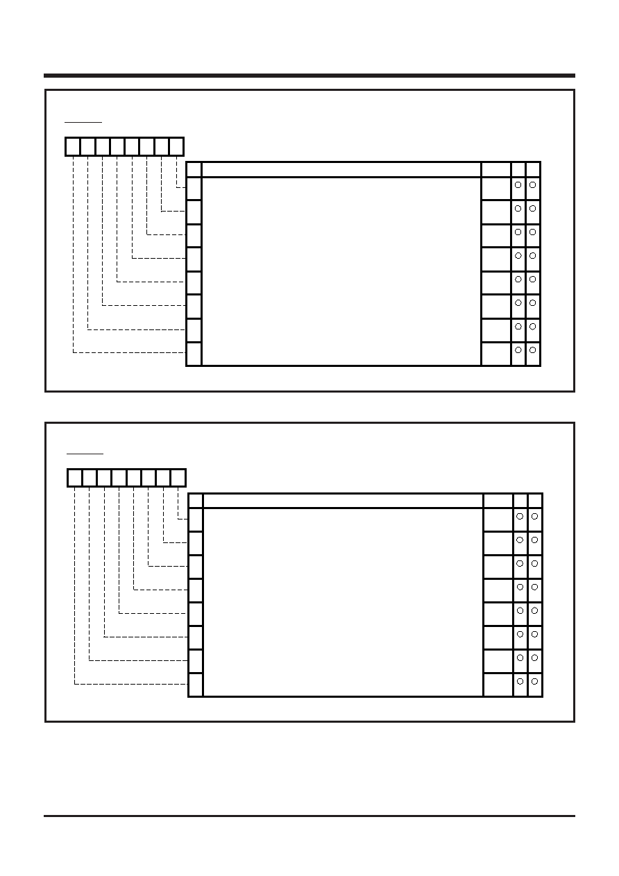
Fig. 3.5.13 Structure of Timer 1
Timer 1
b7 b6 b5 b4 b3 b2 b1 b0
B
Function
At reset
RW
0
1
2
3
4
5
6
7
1
0
Timer 1 (T1) [Address : 29 16]
Set a count value of timer 1.
The value set in this register is written to both timer 1 and timer 1
latch at the same time.
When this register is read out, the timer 1’s count value is read
out.
Timer 2
b7 b6 b5 b4 b3 b2 b1 b0
B
Function
At reset
RW
0
1
2
3
4
5
6
7
0
Timer 2 (T2) [Address : 2A 16]
Set a count value of timer 2.
The value set in this register is written to both timer 2 and timer 2
latch at the same time.
When this register is read out, the timer 2’s count value is read
out.
Fig. 3.5.14 Structure of Timer 2
相關PDF資料 |
PDF描述 |
|---|---|
| M37531E4T-XXXGP | 8-BIT, OTPROM, 8 MHz, MICROCONTROLLER, PQFP32 |
| M37531M4V-XXXGP | 8-BIT, MROM, 8 MHz, MICROCONTROLLER, PQFP32 |
| M37531RSS | 8-BIT, 8 MHz, MICROCONTROLLER, CDIP42 |
| M37532E8FP | 8-BIT, OTPROM, 6 MHz, MICROCONTROLLER, PDSO36 |
| M37532M4-XXXGP | 8-BIT, MROM, 6 MHz, MICROCONTROLLER, PQFP32 |
相關代理商/技術參數(shù) |
參數(shù)描述 |
|---|---|
| M37531E8SP | 制造商:MITSUBISHI 制造商全稱:Mitsubishi Electric Semiconductor 功能描述:SINGLE-CHIP 8-BIT CMOS MICROCOMPUTER |
| M37531M4 | 制造商:MITSUBISHI 制造商全稱:Mitsubishi Electric Semiconductor 功能描述:SINGLE-CHIP 8-BIT CMOS MICROCOMPUTER |
| M37531M4-606SP | 制造商:MITSUBISHI 制造商全稱:Mitsubishi Electric Semiconductor 功能描述:SINGLE-CHIP 8-BIT CMOS MICROCOMPUTER |
| M37531M4-680FP | 制造商:MITSUBISHI 制造商全稱:Mitsubishi Electric Semiconductor 功能描述:SINGLE-CHIP 8-BIT CMOS MICROCOMPUTER |
| M37531M4-680FP-T4 | 制造商:MITSUBISHI 制造商全稱:Mitsubishi Electric Semiconductor 功能描述:SINGLE-CHIP 8-BIT CMOS MICROCOMPUTER |
發(fā)布緊急采購,3分鐘左右您將得到回復。