- 您現(xiàn)在的位置:買賣IC網(wǎng) > PDF目錄45008 > LX1910-CDUT (MICROSEMI CORP-ANALOG MIXED SIGNAL GROUP) 0.8 A SWITCHING REGULATOR, 1325 kHz SWITCHING FREQ-MAX, PDSO8 PDF資料下載
參數(shù)資料
| 型號: | LX1910-CDUT |
| 廠商: | MICROSEMI CORP-ANALOG MIXED SIGNAL GROUP |
| 元件分類: | 穩(wěn)壓器 |
| 英文描述: | 0.8 A SWITCHING REGULATOR, 1325 kHz SWITCHING FREQ-MAX, PDSO8 |
| 封裝: | PLASTIC, MSOP-8 |
| 文件頁數(shù): | 5/12頁 |
| 文件大?。?/td> | 602K |
| 代理商: | LX1910-CDUT |
LX1910
PRELIMINARY DATA SHEET
Microsemi
Integrated Products Division
11861 Western Avenue, Garden Grove, CA. 92841, 714-898-8121, Fax: 714-893-2570
Page 2
WWW
.Microse
m
i
.CO
M
High Frequency Step Down Regulator
I N T E GR A T ED
PRODUCT S
Copyright
2000
Rev. 0.9a, 2004-04-16
ABSOLUTE MAXIMUM RATINGS
Supply Input Voltage (IN) ...................................................................-0.3V to 7V
FB Input Voltage .................................................................................-0.3V to 2V
SW Voltage.......................................................................... -0.3V to (VIN + 0.3V)
SW Peak Current (Internally Limited)...............................................................1A
SHDN Input Voltage ............................................................................-0.3V to 7V
Operating Temperature Range .......................................................-40
°C to 125°C
Maximum Junction Temperature ................................................................. 150
°C
Storage Temperature Range...........................................................-65
°C to 150°C
Lead Temperature (Soldering 40 seconds) .................................................. 250
°C
Note: Exceeding these ratings could cause damage to the device. All voltages are with respect to
Ground. Currents are positive into, negative out of specified terminal
.
x denotes respective pin designator 1, 2, or 3
TH ERMAL DATA
DU Plastic MSOP 8-Pin
THERMAL RESISTANCE
-JUNCTION TO AMBIENT,
θ
JA
206
°C/W
Junction Temperature Calculation: TJ = TA + (PD x θJA).
The
θJA numbers are guidelines for the thermal performance of the device/pc-board system. All of the
above assume no ambient airflow.
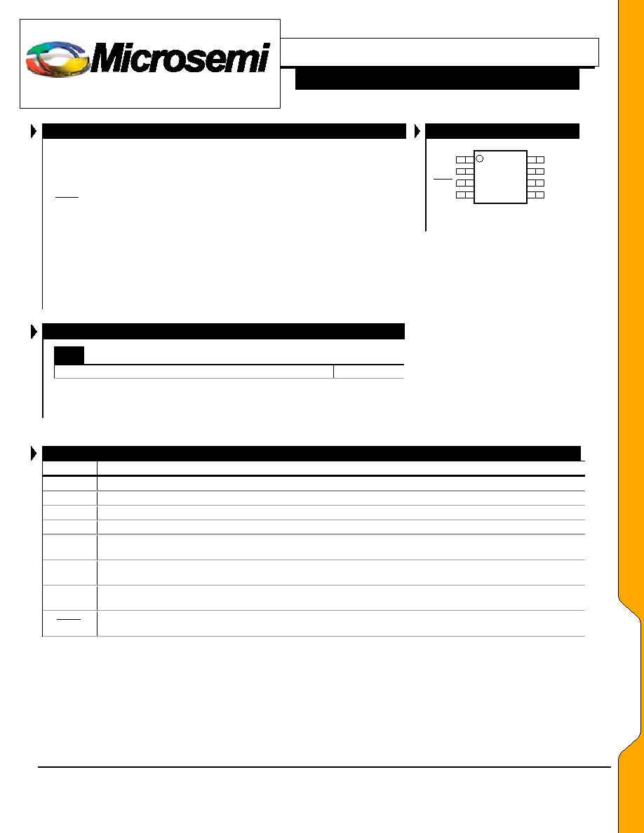
PACKAGE PIN OUT
PVIN
AVIN
SHDN
COMP
FB
AGND
PGND
SW
1
2
3
4
5
6
7
8
DU PACKAGE
(Top View)
FUNCTIONAL PIN DESCRIPTION
Name
Description
SW
Switch Node Connection – Connects to the internal P-Channel MOSFET drain.
AGND
Analog Circuit Ground – Common ground reference for IC operation.
PGND
Power Ground Return – Return for the internal P-Channel MOSFET gate driver.
FB
Feedback Error Amplifier Input – Connect to the output voltage through a resistor divider.
PVIN
MOSFET Source Supply – Connected to the internal P-Channel MOSFET Source. Connect to an unregulated
supply voltage.
AVIN
IC Input Voltage Supply – Supplies power to the regulator circuitry. Connect to an unregulated supply voltage
with adequate decoupling.
COMP
Error Amplifier Output – Loop compensation is effected by placing a series resistor/capacitor combination
between the COMP pin and AGND.
SHDN
Enable Signal Input – Active low signal which places the IC in a shutdown mode, reducing quiescent current to
less than 1
A. In shutdown mode, pin 8 (SW) becomes high impedance.
PP
AA
CC
KK
AA
GG
EE
DD
AA
TT
AA
相關(guān)PDF資料 |
PDF描述 |
|---|---|
| LX2202CLQ-TR | 1-CHANNEL POWER SUPPLY SUPPORT CKT, PQCC20 |
| LX2208ILD-TR | 1-CHANNEL POWER SUPPLY SUPPORT CKT, PDSO12 |
| LX432ISET | 1-OUTPUT TWO TERM VOLTAGE REFERENCE, 1.24 V, PDSO5 |
| LX432CSET | 1-OUTPUT TWO TERM VOLTAGE REFERENCE, 1.24 V, PDSO5 |
| LX432CSCT | 1-OUTPUT TWO TERM VOLTAGE REFERENCE, 1.24 V, PDSO3 |
相關(guān)代理商/技術(shù)參數(shù) |
參數(shù)描述 |
|---|---|
| LX1911 | 制造商:MICROSEMI 制造商全稱:Microsemi Corporation 功能描述:1.5A, 1.1MHZ PWM Step-Down Regulator |
| LX1911CLD | 制造商:Microsemi Corporation 功能描述:DC:DC CONVERTER - Bulk |
| LX1912 | 制造商:MICROSEMI 制造商全稱:Microsemi Corporation 功能描述:VREF @ 800mV, 1.0A, 1.2MHz PWM Current Mode PWM Buck regulator |
| LX1912 EVAL KIT | 制造商:Microsemi Corporation 功能描述:DC:DC CONVERTER - Bulk |
| LX1912CSG | 制造商:Microsemi Corporation 功能描述:PWM CONTROLLERS - Bulk |
發(fā)布緊急采購,3分鐘左右您將得到回復(fù)。