- 您現(xiàn)在的位置:買賣IC網(wǎng) > PDF目錄45008 > LX1692BIPW-TR (MICROSEMI CORP-ANALOG MIXED SIGNAL GROUP) 0.1 A SWITCHING CONTROLLER, PDSO20 PDF資料下載
參數(shù)資料
| 型號: | LX1692BIPW-TR |
| 廠商: | MICROSEMI CORP-ANALOG MIXED SIGNAL GROUP |
| 元件分類: | 穩(wěn)壓器 |
| 英文描述: | 0.1 A SWITCHING CONTROLLER, PDSO20 |
| 封裝: | ROHS COMPLIANT, PLASTIC, TSSOP-20 |
| 文件頁數(shù): | 6/13頁 |
| 文件大?。?/td> | 300K |
| 代理商: | LX1692BIPW-TR |
LX1692B
PRODUCTION DATA SHEET
Microsemi
Integrated Products Division
11861 Western Avenue, Garden Grove, CA. 92841, 714-898-8121, Fax: 714-893-2570
Page 2
Copyright
2005
Rev. 1.1, 12/20/2006
WWW
.Microse
m
i
.CO
M
Full Bridge Resonant CCFL Controller
TM
ABSOLUTE MAXIMUM RATINGS
Supply Input Voltage(VDDP)........................................................................................ 6V
VIN_SNS
..................................................................................... -0.3V to VDDP+0.5V
Digital Input (ENABLE)................................................................. -0.3V to VDDP+0.5V
Analog Inputs (ISNS, OV_SNS, OC_SNS)clamped to ±14V Max Peak Current ±100mA
Analog Inputs (BRITE_A, BRITE_D)........................................... -0.3V to VDDP +0.5V
Digital Outputs (AOUT, BOUT, COUT, DOUT).......................... -0.3V to VDDP +0.5V
Analog Outputs (I_R, ICOMP, VCOMP) ..................................... -0.3V to VDDP + 0.5V
Maximum Operating Junction Temperature .............................................................150°C
Storage Temperature Range........................................................................... -65 to 150°C
Peak Package Solder Reflow Temp. (40 seconds maximum exposure)........260°C(+0, -5)
Note: Exceeding these ratings could cause damage to the device. All voltages are with respect
to
Ground. Currents are positive into, negative out of specified terminal
.
TH ERMAL DATA
DW Plastic SOIC 20-Pin
THERMAL RESISTANCE
-JUNCTION TO AMBIENT,
θ
JA
85
°C/W
PW Plastic TSSOP 20-Pin
THERMAL RESISTANCE
-JUNCTION TO AMBIENT,
θ
JA
99
°C/W
Junction Temperature Calculation: TJ = TA + (PD x θJA).
The
θ
JA numbers are guidelines for the thermal performance of the device/pc-board system. All of the
above assume no ambient airflow.
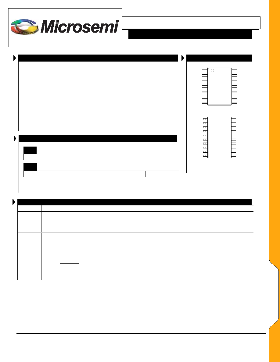
PACKAGE PIN OUT
C_R
I_R
C_BST
C_TO
VDDA
ENABLE
BRITE_D
ICOMP
VIN_SNS
OC_SNS
OV_SNS
ISNS
DOUT
COUT
BOUT
AOUT
1
10
11
20
VCOMP
BRITE_A
GND
VDDP
PW PACKAGE
(Top View)
1
10
11
20
9
8
7
6
5
4
3
2
12
13
14
15
16
17
18
19
C_R
I_R
C_BST
C_TO
VDDA
ENABLE
BRITE_D
ICOMP
VCOMP
BRITE_A
VIN_SNS
OC_SNS
OV_SNS
ISNS
DOUT
COUT
BOUT
AOUT
GND
VDDP
DW PACKAGE
(Top View)
RoHS / Pb-free 100% Matte Tin Lead Finish
FUNCTIONAL PIN DESCRIPTION
Name
Description
C_R
Lamp Frequency Programming Capacitor Pin – lamp running frequency is set by the combination of C_R and
I_R. The internal lamp current oscillator frequency can be forced to follow an external clock signal at this pin. In
this case, the programmed frequency must be lower than the external frequency. Minimum pulse width for
external synch signal is 1sec. Maximum duty is 50%
I_R
Current Reference Resistor Input. Connects to an external resistor that determines the magnitude of the
internal bias currents. The I_R pin is a DC reference voltage of 1V. This voltage should only be used for its
intended function. The reference current established at this pin, by connecting an external resistor, is used to
charge a capacitor at the C_R pin. The nominal lamp frequency can be adjusted by varying this resistor value in
the range of 20K to 100K Ohms. (Note: C is in pF, R is in
Ω
K
, Freq is in kHz).
R
_
I
R
_
C
3
LAMP
R
C
10
242
F
×
=
Other reference currents derived from I_R are used for the digital dimming burst oscillator and the strike time
out function.
PP
AA
CC
KK
AA
GG
EE
DD
AA
TT
AA
相關(guān)PDF資料 |
PDF描述 |
|---|---|
| LX1692IDW-TR | 0.1 A SWITCHING CONTROLLER, PDSO20 |
| LX1732CDUTR | 1 A SWITCHING REGULATOR, 135 kHz SWITCHING FREQ-MAX, PDSO8 |
| LX1732CDU-TR | 1 A SWITCHING REGULATOR, 135 kHz SWITCHING FREQ-MAX, PDSO8 |
| LX1741CDUT | 0.145 A SWITCHING CONTROLLER, PDSO8 |
| LX1742CDU-TR | SWITCHING REGULATOR, PDSO8 |
相關(guān)代理商/技術(shù)參數(shù) |
參數(shù)描述 |
|---|---|
| LX1692EIDW | 制造商:Microsemi Corporation 功能描述:CCFL BACKLIGHT CONTROLLER IC - Bulk |
| LX1692F | 制造商:MICROSEMI 制造商全稱:Microsemi Corporation 功能描述:TM Full Bridge Resonant CCFL Controller |
| LX1692FIDW | 制造商:Microsemi Corporation 功能描述:CCFL BACKLIGHT CONTROLLER IC - Bulk |
| LX1692FIDW-TR | 制造商:Microsemi Corporation 功能描述:CCFL BACKLIGHT CONTROLLER IC - Tape and Reel |
| LX1692FIPW | 制造商:Microsemi Corporation 功能描述:CCFL BACKLIGHT CONTROLLER IC - Bulk |
發(fā)布緊急采購,3分鐘左右您將得到回復(fù)。