- 您現在的位置:買賣IC網 > PDF目錄45002 > LW016BK1 (LINEAGE POWER LLC) 2-OUTPUT 16 W DC-DC REG PWR SUPPLY MODULE PDF資料下載
參數資料
| 型號: | LW016BK1 |
| 廠商: | LINEAGE POWER LLC |
| 元件分類: | 電源模塊 |
| 英文描述: | 2-OUTPUT 16 W DC-DC REG PWR SUPPLY MODULE |
| 封裝: | MODULE-9 |
| 文件頁數: | 12/16頁 |
| 文件大?。?/td> | 486K |
| 代理商: | LW016BK1 |
Lineage Power
5
Advance Data Sheet
April 2008
36 Vdc to 75 Vdc Inputs; 16 W
LW016 Dual-Output-Series Power Modules:
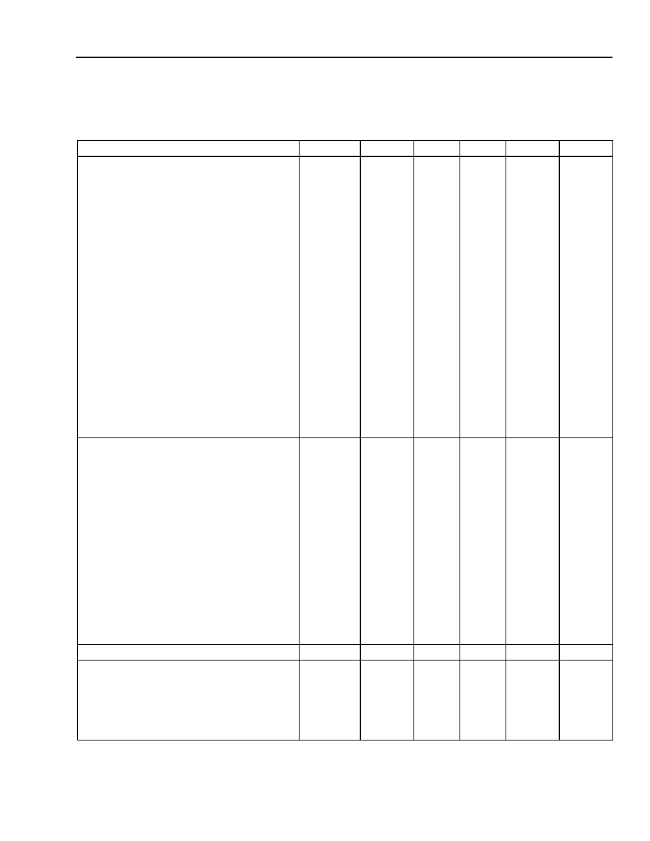
Feature Specifications
Unless otherwise indicated, specifications apply over all operating input voltage, resistive load, and temperature
conditions. See Feature Descriptions and Design Considerations for further information.
Parameter
Device
Symbol
Min
Typ
Max
Unit
Remote On/Off Signal Interface:
(VI = 0 V to VI, max; open collector or
equivalent compatible; signal referenced to
Descriptions.):
Negative Logic (Device Code Suffix “1”):
Logic Low—Module On
Logic High—Module Off
Positive Logic (If Device Code Suffix “1” is
not specified):
Logic Low—Module Off
Logic High—Module On
Module Specifications:
On/Off Current—Logic Low
On/Off Voltage:
Logic Low
Logic High (Ion/off = 0)
Open Collector Switch Specifications:
Leakage Current During Logic High
(Von/off = 6 V)
Output Low Voltage During Logic Low
(Ion/off = 1 mA)
All
Ion/off
Von/off
Ion/off
Von/off
—
–0.7
—
1.0
1.2
6
50
1.2
mA
V
A
V
Turn-on Delay and Rise Times
(at 80% of IO, max; TA = 25 °C):
Case 1: On/Off Input Is Set for Unit On and
Then Input Power Is Applied (delay from
point at which VI = 48 V until VO = 10% of
VO, nom).
Case 2: 48 V Input Is Applied for at Least
One Second, and Then the On/Off Input
Is Set to Turn the Module On (delay from
point at which on/off input is toggled until
VO = 10% of VO, nom).
Output Voltage Rise Time (time for VO to
rise from 10% of VO, nom to 90% of VO,
nom
)
Output Voltage Overshoot
(at 80% of IO, max; TA = 25 °C)
All
Tdelay
Trise
—
27
3
1
—
50
10
3.0
5
ms
%
Output Voltage Set-point Adjustment Range
All
—
90
—
110
%VO, nom
Output Overvoltage Protection (clamp)
LW016AJ
LW016BK
LW016CL
VO1, clamp
VO2, clamp
VO1, clamp
VO2, clamp
VO1, clamp
VO2, clamp
5.6
–5.6
13.2
–13.2
16.5
–16.5
—
7.0
–7.0
16.5
–16.5
19.0
–19.0
V
相關PDF資料 |
PDF描述 |
|---|---|
| LW016AJ7 | 2-OUTPUT 16 W DC-DC REG PWR SUPPLY MODULE |
| LW016AJ1 | 2-OUTPUT 16 W DC-DC REG PWR SUPPLY MODULE |
| LW016BK8 | 2-OUTPUT 16 W DC-DC REG PWR SUPPLY MODULE |
| LW016AJ3 | 2-OUTPUT 16 W DC-DC REG PWR SUPPLY MODULE |
| LW016BK3 | 2-OUTPUT 16 W DC-DC REG PWR SUPPLY MODULE |
相關代理商/技術參數 |
參數描述 |
|---|---|
| LW016BK3 | 制造商:未知廠家 制造商全稱:未知廠家 功能描述:Analog IC |
| LW016BK7 | 制造商:未知廠家 制造商全稱:未知廠家 功能描述:Analog IC |
| LW016BK8 | 制造商:未知廠家 制造商全稱:未知廠家 功能描述:Analog IC |
| LW016CL | 制造商:未知廠家 制造商全稱:未知廠家 功能描述:DC-to-DC Voltage Converter |
| LW016CL1 | 制造商:未知廠家 制造商全稱:未知廠家 功能描述:Analog IC |
發(fā)布緊急采購,3分鐘左右您將得到回復。