- 您現(xiàn)在的位置:買賣IC網(wǎng) > PDF目錄45001 > LTM9005CV-AB#PBF (LINEAR TECHNOLOGY CORP) SPECIALTY ANALOG CIRCUIT, PBGA204 PDF資料下載
參數(shù)資料
| 型號: | LTM9005CV-AB#PBF |
| 廠商: | LINEAR TECHNOLOGY CORP |
| 元件分類: | 模擬信號調(diào)理 |
| 英文描述: | SPECIALTY ANALOG CIRCUIT, PBGA204 |
| 封裝: | 22 X 15 MM, 4.32 MM HEIGHT, LEAD FREE, MO-222, LGA-204 |
| 文件頁數(shù): | 24/24頁 |
| 文件大?。?/td> | 468K |
| 代理商: | LTM9005CV-AB#PBF |
LTM9005
9
9005p
pin FuncTions
RF (Pin M3): Single-Ended Input for the RF Signal. This
pin is internally connected to the primary side of the RF
input transformer, which has low DC resistance to ground.
If the RF source is not DC blocked, then a series blocking
capacitor must be used. The RF input is internally matched
from 1.6GHz to 2.3GHz. Operation down to 400MHz or up
to 3.8GHz is possible with simple external matching.
LO (Pin M6): Single-Ended Input for the Local Oscillator
Signal. This pin is internally connected to the primary side
of the LO transformer, which is internally DC blocked. An
external blocking capacitor is not required. The LO input
is internally matched from 1GHz to 5GHz. Operation down
to 380MHz is possible with simple external matching.
GAIN (Pin F1): Cathode of PIN Diode. Sinking current
from GAIN attenuates the signal. The forward voltage is
approximately 1V and the output impedance is 50Ω.
EN (Pin H1): Mixer Enable Pin. Connecting EN to VCC1
resultsinnormaloperation.ConnectingENtoGNDdisables
the mixer. The EN pin should not be left floating.
AMP1SHDN(PinD4),AMP2SHDN(PinL16):AmplifierEn-
ablePins.ConnectingAMPSHDNtoGNDresultsinnormal
operation. Connecting AMP1SHDN to VCC2 disables the
amplifier preceding the SAW filter and connecting AMP-
2SHDN to VCC3 disables the amplifier following the SAW
filter. It is recommended to tie AMP1SHDN, AMP2SHDN
and ADCSHDN together and control with 3V logic.
CLK (Pin A11): ADC Clock Input. The input sample starts
on the positive edge.
ADCSHDN (Pin C13): ADC Shutdown Mode Selection Pin.
Connecting ADCSHDN to GND and OE to GND results in
normal operation with the ADC outputs enabled. Connect-
ing ADCSHDN to GND and OE to VDD results in normal
operation with the outputs at high impedance. Connecting
ADCSHDN to VDD and OE to GND results in nap mode with
the outputs at high impedance. Connecting ADCSHDN to
VDD and OE to VDD results in sleep mode with the outputs
at high impedance.
OE (Pin C12): Output Enable Pin. Refer to ADCSHDN pin
function.
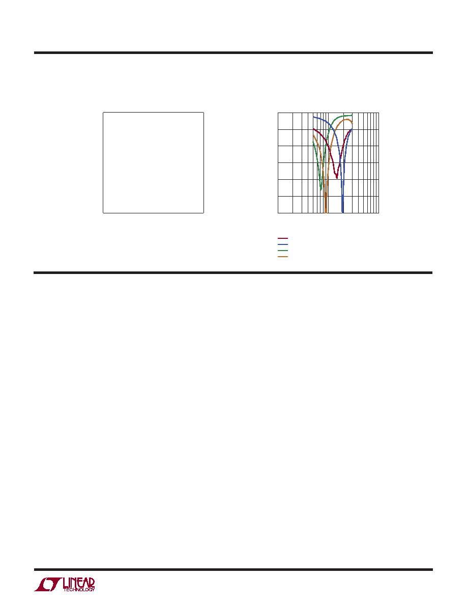
Typical perForMance characTerisTics
LTM9005: RF Port Impedance
LTM9005: RF Port Return Loss
vs Frequency
FREQUENCY (MHz)
RETURN
LOSS
(dB)
9005 G10
0
–30
–25
–20
–15
–10
–5
100
1000
10000
NO MATCHING ELEMENTS
1.95GHz MATCH (5.6nH)
700MHz MATCH (4.7pF)
900MHz MATCH (2.7pF)
相關PDF資料 |
PDF描述 |
|---|---|
| LTM9005IV-AB#PBF | SPECIALTY ANALOG CIRCUIT, PBGA204 |
| LUCW3000ACN-TR | PLL FREQUENCY SYNTHESIZER, 2200 MHz, PDSO14 |
| LUCW3000ACN | PLL FREQUENCY SYNTHESIZER, 2200 MHz, PDSO14 |
| LUCW3000ACN | PLL FREQUENCY SYNTHESIZER, 2200 MHz, PDSO14 |
| LUCW3000CCN | PLL FREQUENCY SYNTHESIZER, 2200 MHz, PDSO14 |
相關代理商/技術參數(shù) |
參數(shù)描述 |
|---|---|
| LTM9005GD | 功能描述:LED 電路板指示器 Vert LED Assmbly 5mm Green RoHS:否 制造商:Lumex LED 大小:3 mm 照明顏色:Green 波長:565 nm 光強度:30 mcd 安裝類型:SMD/SMT 顯示角:60 deg 封裝:Reel |
| LTM9006-14 | 制造商:LINER 制造商全稱:Linear Technology 功能描述:14-Bit, 65Msps/40Msps/25Msps Low Power Octal ADCs |
| LTM9006CY-14#PBF | 制造商:Linear Technology 功能描述:IC ADC 14BIT SPI/SRL 25M 140-BGA 制造商:Linear Technology 功能描述:ADC 8CH 1.8V 14BIT 25MSPS 制造商:Linear Technology 功能描述:ADC, 14BIT, 25MSPS, SPI, BGA-140; Resolution (Bits):14bit; Sampling Rate:25MSPS; Supply Voltage Type:Single; Supply Voltage Min:1.7V; Supply Voltage Max:1.9V; Supply Current:175mA; Digital IC Case Style:BGA; No. of Pins:140 ;RoHS Compliant: Yes |
| LTM9006IY-14#PBF | 制造商:Linear Technology 功能描述:IC ADC 14BIT SPI/SRL 25M 140-BGA 制造商:Linear Technology 功能描述:MS-uModule, 14-bit, 25Msps, 1.8V Octal ADC, Serial LVDS Outputs |
| LTM9007-14 | 制造商:LINER 制造商全稱:Linear Technology 功能描述:14-Bit, 65Msps/40Msps/25Msps Low Power Octal ADCs |
發(fā)布緊急采購,3分鐘左右您將得到回復。