- 您現(xiàn)在的位置:買賣IC網(wǎng) > PDF目錄44995 > LTC3890HUH#PBF (LINEAR TECHNOLOGY CORP) DUAL SWITCHING CONTROLLER, 585 kHz SWITCHING FREQ-MAX, PQCC32 PDF資料下載
參數(shù)資料
| 型號(hào): | LTC3890HUH#PBF |
| 廠商: | LINEAR TECHNOLOGY CORP |
| 元件分類: | 穩(wěn)壓器 |
| 英文描述: | DUAL SWITCHING CONTROLLER, 585 kHz SWITCHING FREQ-MAX, PQCC32 |
| 封裝: | 5 X 5 MM, 0.75 MM HEIGHT, LEAD FREE, PLASTIC, MO-220WHHD, QFN-32 |
| 文件頁數(shù): | 11/38頁 |
| 文件大?。?/td> | 381K |
| 代理商: | LTC3890HUH#PBF |
第1頁第2頁第3頁第4頁第5頁第6頁第7頁第8頁第9頁第10頁當(dāng)前第11頁第12頁第13頁第14頁第15頁第16頁第17頁第18頁第19頁第20頁第21頁第22頁第23頁第24頁第25頁第26頁第27頁第28頁第29頁第30頁第31頁第32頁第33頁第34頁第35頁第36頁第37頁第38頁
LTC3890
19
3890fa
APPLICATIONS INFORMATION
RMS capacitor current requirement. Increasing the out-
put current drawn from the other controller will actually
decrease the input RMS ripple current from its maximum
value. The out-of-phase technique typically reduces the
input capacitor’s RMS ripple current by a factor of 30%
to 70% when compared to a single phase power supply
solution.
In continuous mode, the source current of the top MOSFET
is a square wave of duty cycle (VOUT)/(VIN). To prevent
large voltage transients, a low ESR capacitor sized for the
maximum RMS current of one channel must be used. The
maximum RMS capacitor current is given by:
CIN Required IRMS ≈
IMAX
VIN
VOUT
() VIN –VOUT
()
1/ 2
(1)
This formula has a maximum at VIN = 2VOUT, where IRMS
= IOUT/2. This simple worst-case condition is commonly
used for design because even significant deviations do not
offer much relief. Note that capacitor manufacturers’ ripple
current ratings are often based on only 2000 hours of life.
This makes it advisable to further derate the capacitor, or
to choose a capacitor rated at a higher temperature than
required. Several capacitors may be paralleled to meet
size or height requirements in the design. Due to the high
operating frequency of the LTC3890, ceramic capacitors
can also be used for CIN. Always consult the manufacturer
if there is any question.
The benefit of the LTC3890 2-phase operation can be cal-
culated by using Equation 1 for the higher power controller
and then calculating the loss that would have resulted if
both controller channels switched on at the same time.
The total RMS power lost is lower when both controllers
are operating due to the reduced overlap of current pulses
required through the input capacitor’s ESR. This is why
the input capacitor’s requirement calculated above for the
worst-case controller is adequate for the dual controller
design. Also, the input protection fuse resistance, battery
resistance, and PC board trace resistance losses are also
reduced due to the reduced peak currents in a 2-phase
system. The overall benefit of a multiphase design will
only be fully realized when the source impedance of the
power supply/battery is included in the efficiency testing.
The drains of the top MOSFETs should be placed within
1cm of each other and share a common CIN(s). Separating
the drains and CIN may produce undesirable voltage and
current resonances at VIN.
A small (0.1μF to 1μF) bypass capacitor between the chip
VIN pin and ground, placed close to the LTC3890, is also
suggested. A 10Ω resistor placed between CIN (C1) and
the VIN pin provides further isolation between the two
channels.
The selection of COUT is driven by the effective series
resistance (ESR). Typically, once the ESR requirement
is satisfied, the capacitance is adequate for filtering. The
output ripple (ΔVOUT) is approximated by:
ΔVOUT ≈ΔIL ESR +
1
8 f COUT
where f is the operating frequency, COUT is the output
capacitance and ΔIL is the ripple current in the inductor.
The output ripple is highest at maximum input voltage
since ΔIL increases with input voltage.
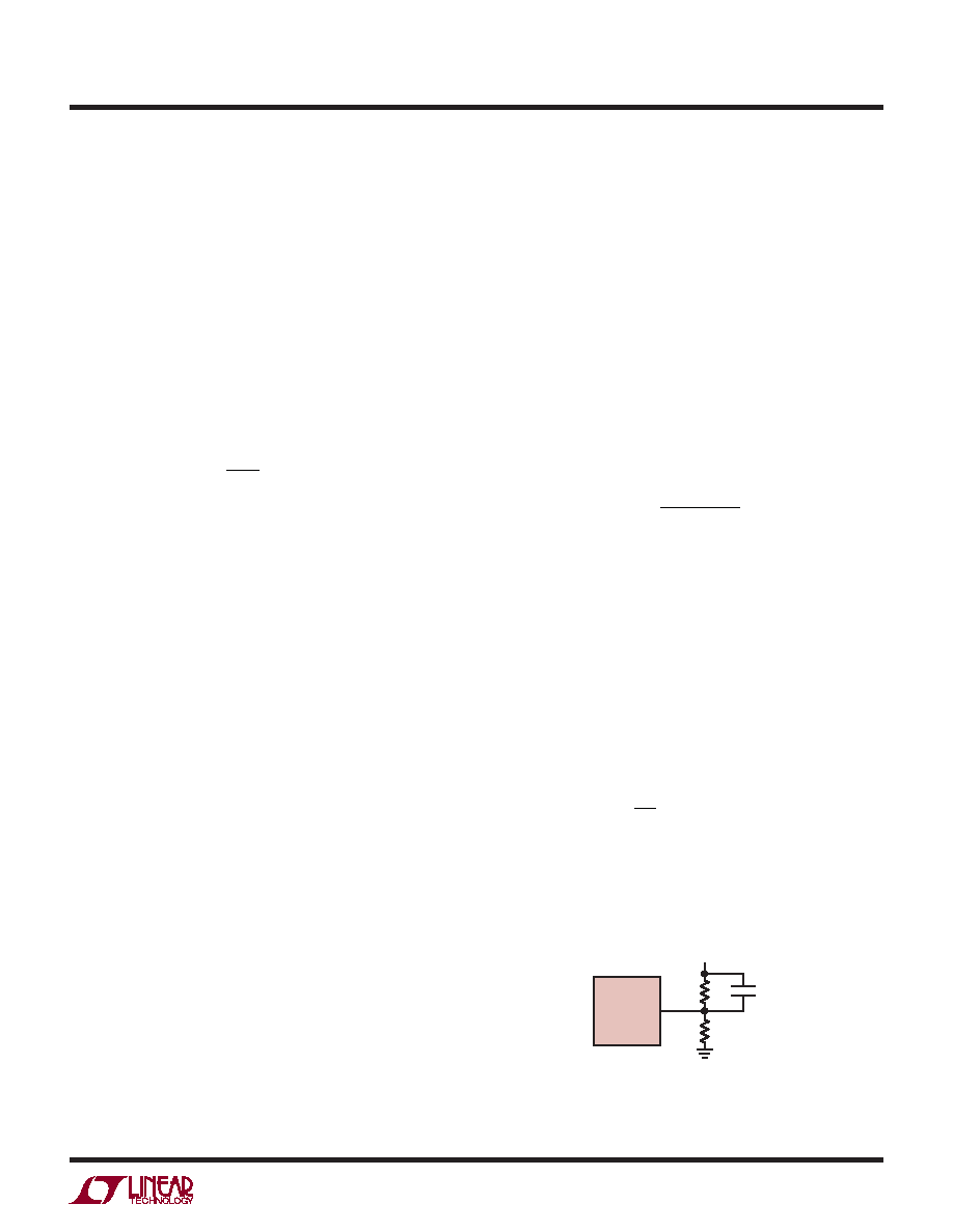
Setting Output Voltage
The LTC3890 output voltages are each set by an external
feedback resistor divider carefully placed across the out-
put, as shown in Figure 5. The regulated output voltage
is determined by:
VOUT = 0.8V 1+
RB
RA
To improve the frequency response, a feedforward ca-
pacitor, CFF, may be used. Great care should be taken to
route the VFB line away from noise sources, such as the
inductor or the SW line.
1/2 LTC3890
VFB
VOUT
RB
CFF
RA
3890 F05
Figure 5. Setting Output Voltage
相關(guān)PDF資料 |
PDF描述 |
|---|---|
| LTC3890HUH#TRPBF | DUAL SWITCHING CONTROLLER, 585 kHz SWITCHING FREQ-MAX, PQCC32 |
| LTC3891HFE#TRPBF | SWITCHING CONTROLLER, 900 kHz SWITCHING FREQ-MAX, PDSO20 |
| LTC3891HUDC#TRPBF | SWITCHING CONTROLLER, 900 kHz SWITCHING FREQ-MAX, PQCC20 |
| LTC3891MPFE#TRPBF | SWITCHING CONTROLLER, 900 kHz SWITCHING FREQ-MAX, PDSO20 |
| LTC3891MPUDC#PBF | SWITCHING CONTROLLER, 900 kHz SWITCHING FREQ-MAX, PQCC20 |
相關(guān)代理商/技術(shù)參數(shù) |
參數(shù)描述 |
|---|---|
| LTC3890IGN-1#PBF | 功能描述:IC REG CTRLR BUCK PWM CM 28-SSOP RoHS:是 類別:集成電路 (IC) >> PMIC - 穩(wěn)壓器 - DC DC 切換控制器 系列:PolyPhase® 標(biāo)準(zhǔn)包裝:4,500 系列:PowerWise® PWM 型:控制器 輸出數(shù):1 頻率 - 最大:1MHz 占空比:95% 電源電壓:2.8 V ~ 5.5 V 降壓:是 升壓:無 回掃:無 反相:無 倍增器:無 除法器:無 Cuk:無 隔離:無 工作溫度:-40°C ~ 125°C 封裝/外殼:6-WDFN 裸露焊盤 包裝:帶卷 (TR) 配用:LM1771EVAL-ND - BOARD EVALUATION LM1771 其它名稱:LM1771SSDX |
| LTC3890IGN-1#TRPBF | 功能描述:IC REG CTRLR BUCK PWM CM 28-SSOP RoHS:是 類別:集成電路 (IC) >> PMIC - 穩(wěn)壓器 - DC DC 切換控制器 系列:PolyPhase® 標(biāo)準(zhǔn)包裝:4,500 系列:PowerWise® PWM 型:控制器 輸出數(shù):1 頻率 - 最大:1MHz 占空比:95% 電源電壓:2.8 V ~ 5.5 V 降壓:是 升壓:無 回掃:無 反相:無 倍增器:無 除法器:無 Cuk:無 隔離:無 工作溫度:-40°C ~ 125°C 封裝/外殼:6-WDFN 裸露焊盤 包裝:帶卷 (TR) 配用:LM1771EVAL-ND - BOARD EVALUATION LM1771 其它名稱:LM1771SSDX |
| LTC3890IGN-3#PBF | 制造商:Linear Technology 功能描述:IC REG CTRLR BUCK PWM CM 28SSOP 制造商:Linear Technology 功能描述:DC-DC CONTROLLER BUCK 900KHZ 制造商:Linear Technology 功能描述:BUCK DUAL CNTRL 4-60V 850K 制造商:Linear Technology 功能描述:DC-DC CONTROLLER, BUCK, 900KHZ, SSOP-28 制造商:Linear Technology 功能描述:DC-DC CONTROLLER, BUCK, 900KHZ, SSOP-28; Primary Input Voltage:60V; No. of Outputs:2; No. of Pins:28; Operating Temperature Min:-40C; Operating Temperature Max:125C; Operating Temperature Range:-40C to +125C ;RoHS Compliant: Yes |
| LTC3890IGN-3#TRPBF | 制造商:Linear Technology 功能描述:IC REG CTRLR BUCK PWM CM 28SSOP |
| LTC3890IUH#PBF | 功能描述:IC REG CTRLR BUCK PWM CM 32-QFN RoHS:是 類別:集成電路 (IC) >> PMIC - 穩(wěn)壓器 - DC DC 切換控制器 系列:PolyPhase® 標(biāo)準(zhǔn)包裝:4,500 系列:PowerWise® PWM 型:控制器 輸出數(shù):1 頻率 - 最大:1MHz 占空比:95% 電源電壓:2.8 V ~ 5.5 V 降壓:是 升壓:無 回掃:無 反相:無 倍增器:無 除法器:無 Cuk:無 隔離:無 工作溫度:-40°C ~ 125°C 封裝/外殼:6-WDFN 裸露焊盤 包裝:帶卷 (TR) 配用:LM1771EVAL-ND - BOARD EVALUATION LM1771 其它名稱:LM1771SSDX |
發(fā)布緊急采購,3分鐘左右您將得到回復(fù)。