- 您現(xiàn)在的位置:買賣IC網 > PDF目錄44992 > LTC3731HUH#PBF (LINEAR TECHNOLOGY CORP) 5 A SWITCHING CONTROLLER, 750 kHz SWITCHING FREQ-MAX, PQCC32 PDF資料下載
參數(shù)資料
| 型號: | LTC3731HUH#PBF |
| 廠商: | LINEAR TECHNOLOGY CORP |
| 元件分類: | 穩(wěn)壓器 |
| 英文描述: | 5 A SWITCHING CONTROLLER, 750 kHz SWITCHING FREQ-MAX, PQCC32 |
| 封裝: | 5 X 5 MM, LEAD FREE, PLASTIC, MO-220WHHD, QFN-32 |
| 文件頁數(shù): | 6/34頁 |
| 文件大小: | 427K |
| 代理商: | LTC3731HUH#PBF |
第1頁第2頁第3頁第4頁第5頁當前第6頁第7頁第8頁第9頁第10頁第11頁第12頁第13頁第14頁第15頁第16頁第17頁第18頁第19頁第20頁第21頁第22頁第23頁第24頁第25頁第26頁第27頁第28頁第29頁第30頁第31頁第32頁第33頁第34頁
LTC3731H
3731Hfb
MOSFET in applications that have an output voltage that
is less than 1/3 of the input voltage. In applications where
VIN >> VOUT, the top MOSFETs’ on-resistance is normally
less important for overall efficiency than its input capaci-
tance at operating frequencies above 300kHz. MOSFET
manufacturershavedesignedspecialpurposedevicesthat
provide reasonably low on-resistance with significantly
reduced input capacitance for the main switch application
in switching regulators.
The peak-to-peak MOSFET gate drive levels are set by the
voltage, VCC, requiring the use of logic-level threshold
MOSFETs in most applications. Pay close attention to the
BVDSS specification for the MOSFETs as well; many of the
logic-level MOSFETs are limited to 30V or less.
Selection criteria for the power MOSFETs include the
on-resistance RDS(ON), input capacitance, input voltage
and maximum output current.
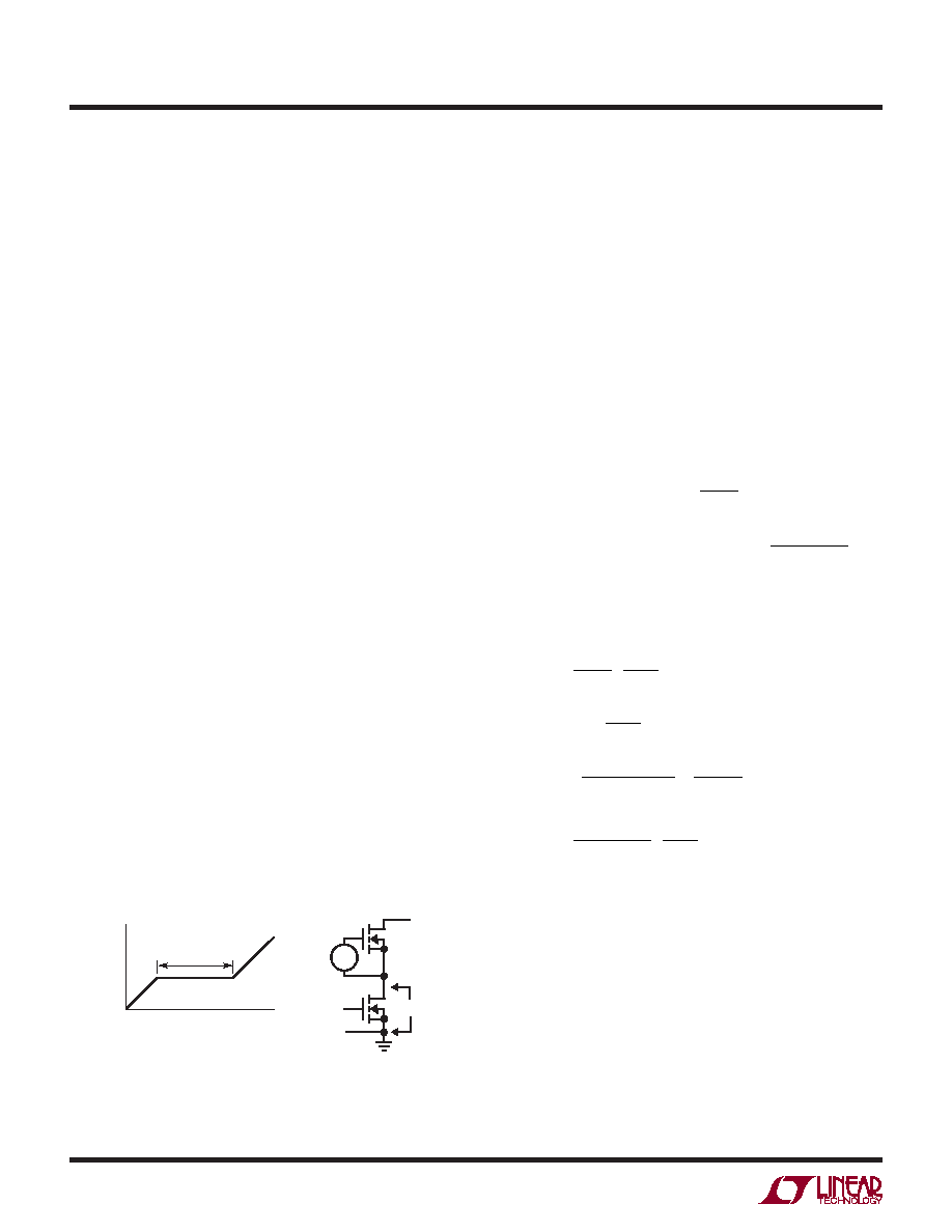
MOSFET input capacitance is a combination of sev-
eral components but can be taken from the typical “gate
charge” curve included on most data sheets (Figure 5).
The curve is generated by forcing a constant input cur-
rent into the gate of a common source, current source
loaded stage and then plotting the gate voltage versus
time. The initial slope is the effect of the gate-to-source
and the gate-to-drain capacitance. The flat portion of the
curve is the result of the Miller multiplication effect of the
drain-to-gate capacitance as the drain drops the voltage
across the current source load. The upper sloping line is
due to the drain-to-gate accumulation capacitance and
the gate-to-source capacitance. The Miller charge (the
increase in coulombs on the horizontal axis from a to b
while the curve is flat) is specified for a given VDS drain
applicaTions inForMaTion
voltage, but can be adjusted for different VDS voltages by
multiplying by the ratio of the application VDS to the curve
specified VDS values. A way to estimate the CMILLER term
is to take the change in gate charge from points a and b
on a manufacturers data sheet and divide by the stated
VDS voltage specified. CMILLER is the most important se-
lection criteria for determining the transition loss term in
the top MOSFET but is not directly specified on MOSFET
data sheets. CRSS and COS are specified sometimes but
definitions of these parameters are not included.
When the controller is operating in continuous mode
the duty cycles for the top and bottom MOSFETs are
given by:
Main SwitchDuty Cycle
V
Synchronous SwitchDuty Cycle
V
OUT
IN
OUT
IN
=
=
–
The power dissipation for the main and synchronous
MOSFETs at maximum output current are given by:
P
V
I
N
R
V
I
N
R
C
V
f
P
V
I
N
R
MAIN
OUT
IN
MAX
DS ON
IN
MAX
DR
MILLER
CC
TH IL
SYNC
IN
OUT
IN
MAX
DS ON
=
+
( )
+
( )(
)
+
( )
=
+
( )
2
1
2
1
d
( )
–
where N is the number of output stages,
d is the tem-
perature dependency of RDS(ON), RDR is the effective top
driverresistance(approximately2ΩatVGS=VMILLER),VIN
is the drain potential and the change in drain potential in
the particular application. VTH(IL) is the data sheet speci-
fied typical gate threshold voltage specified in the power
MOSFET data sheet at the specified drain current. CMILLER
is the calculated capacitance using the gate charge curve
from the MOSFET data sheet and the technique described
above.
Figure 5. Gate Charge Characteristic
+
–
VDS
VIN
3731H F05
VGS
MILLER EFFECT
QIN
a
b
CMILLER = (QB – QA)/VDS
VGS
V
+
–
相關PDF資料 |
PDF描述 |
|---|---|
| LTC3772BETS8#PBF | 1 A SWITCHING CONTROLLER, 650 kHz SWITCHING FREQ-MAX, PDSO8 |
| LTC3772ETS8#PBF | 1 A SWITCHING CONTROLLER, 650 kHz SWITCHING FREQ-MAX, PDSO8 |
| LTC3783IDHD | 1 A SWITCHING CONTROLLER, 1000 kHz SWITCHING FREQ-MAX, PDSO16 |
| LTC3783IFE#TR | 1 A SWITCHING CONTROLLER, 1000 kHz SWITCHING FREQ-MAX, PDSO16 |
| LTC3783IDHD#TR | 1 A SWITCHING CONTROLLER, 1000 kHz SWITCHING FREQ-MAX, PDSO16 |
相關代理商/技術參數(shù) |
參數(shù)描述 |
|---|---|
| LTC3731IG | 制造商:Linear Technology 功能描述:LDO Cntrlr SYNC BUCK REG 0.6V to 6V 36-Pin SSOP |
| LTC3731IG#PBF | 功能描述:IC REG CTRLR BUCK PWM CM 36-SSOP RoHS:是 類別:集成電路 (IC) >> PMIC - 穩(wěn)壓器 - DC DC 切換控制器 系列:PolyPhase® 標準包裝:4,500 系列:PowerWise® PWM 型:控制器 輸出數(shù):1 頻率 - 最大:1MHz 占空比:95% 電源電壓:2.8 V ~ 5.5 V 降壓:是 升壓:無 回掃:無 反相:無 倍增器:無 除法器:無 Cuk:無 隔離:無 工作溫度:-40°C ~ 125°C 封裝/外殼:6-WDFN 裸露焊盤 包裝:帶卷 (TR) 配用:LM1771EVAL-ND - BOARD EVALUATION LM1771 其它名稱:LM1771SSDX |
| LTC3731IG#TRPBF | 功能描述:IC REG CTRLR BUCK PWM CM 36-SSOP RoHS:是 類別:集成電路 (IC) >> PMIC - 穩(wěn)壓器 - DC DC 切換控制器 系列:PolyPhase® 標準包裝:4,500 系列:PowerWise® PWM 型:控制器 輸出數(shù):1 頻率 - 最大:1MHz 占空比:95% 電源電壓:2.8 V ~ 5.5 V 降壓:是 升壓:無 回掃:無 反相:無 倍增器:無 除法器:無 Cuk:無 隔離:無 工作溫度:-40°C ~ 125°C 封裝/外殼:6-WDFN 裸露焊盤 包裝:帶卷 (TR) 配用:LM1771EVAL-ND - BOARD EVALUATION LM1771 其它名稱:LM1771SSDX |
| LTC3731IUH | 制造商:Linear Technology 功能描述:LDO Cntrlr SYNC BUCK REG 0.6V to 6V 32-Pin QFN EP |
| LTC3731IUH#PBF | 功能描述:IC REG CTRLR BUCK PWM CM 32-QFN RoHS:是 類別:集成電路 (IC) >> PMIC - 穩(wěn)壓器 - DC DC 切換控制器 系列:PolyPhase® 標準包裝:4,500 系列:PowerWise® PWM 型:控制器 輸出數(shù):1 頻率 - 最大:1MHz 占空比:95% 電源電壓:2.8 V ~ 5.5 V 降壓:是 升壓:無 回掃:無 反相:無 倍增器:無 除法器:無 Cuk:無 隔離:無 工作溫度:-40°C ~ 125°C 封裝/外殼:6-WDFN 裸露焊盤 包裝:帶卷 (TR) 配用:LM1771EVAL-ND - BOARD EVALUATION LM1771 其它名稱:LM1771SSDX |
發(fā)布緊急采購,3分鐘左右您將得到回復。