- 您現(xiàn)在的位置:買賣IC網(wǎng) > PDF目錄44986 > LT3692IUH#PBF (LINEAR TECHNOLOGY CORP) 5.8 A DUAL SWITCHING CONTROLLER, 2750 kHz SWITCHING FREQ-MAX, PQCC32 PDF資料下載
參數(shù)資料
| 型號: | LT3692IUH#PBF |
| 廠商: | LINEAR TECHNOLOGY CORP |
| 元件分類: | 穩(wěn)壓器 |
| 英文描述: | 5.8 A DUAL SWITCHING CONTROLLER, 2750 kHz SWITCHING FREQ-MAX, PQCC32 |
| 封裝: | 5 X 5 MM, LEAD FREE, PLASTIC, MO-220WHHD, QFN-32 |
| 文件頁數(shù): | 13/36頁 |
| 文件大?。?/td> | 526K |
| 代理商: | LT3692IUH#PBF |
第1頁第2頁第3頁第4頁第5頁第6頁第7頁第8頁第9頁第10頁第11頁第12頁當(dāng)前第13頁第14頁第15頁第16頁第17頁第18頁第19頁第20頁第21頁第22頁第23頁第24頁第25頁第26頁第27頁第28頁第29頁第30頁第31頁第32頁第33頁第34頁第35頁第36頁
LT3692
20
3692f
APPLICATIONS INFORMATION
Shutdown and Undervoltage/Overvoltage Lockout
Typically, undervoltage lockout (UVLO) is used in situa-
tions where the input supply is current limited, or has a
relatively high source resistance. A switching regulator
draws constant power from the source, so source cur-
rent increases as source voltage drops. This looks like a
negative resistance load to the source and can cause the
sourcetocurrentlimitorlatchlowunderlowsourcevoltage
conditions. UVLO prevents the regulator from operating
at source voltages where these problems might occur.
Overvoltage lockout (OVLO) is typically used to shut down
the switching regulator during potentially harmful input
voltage transients.
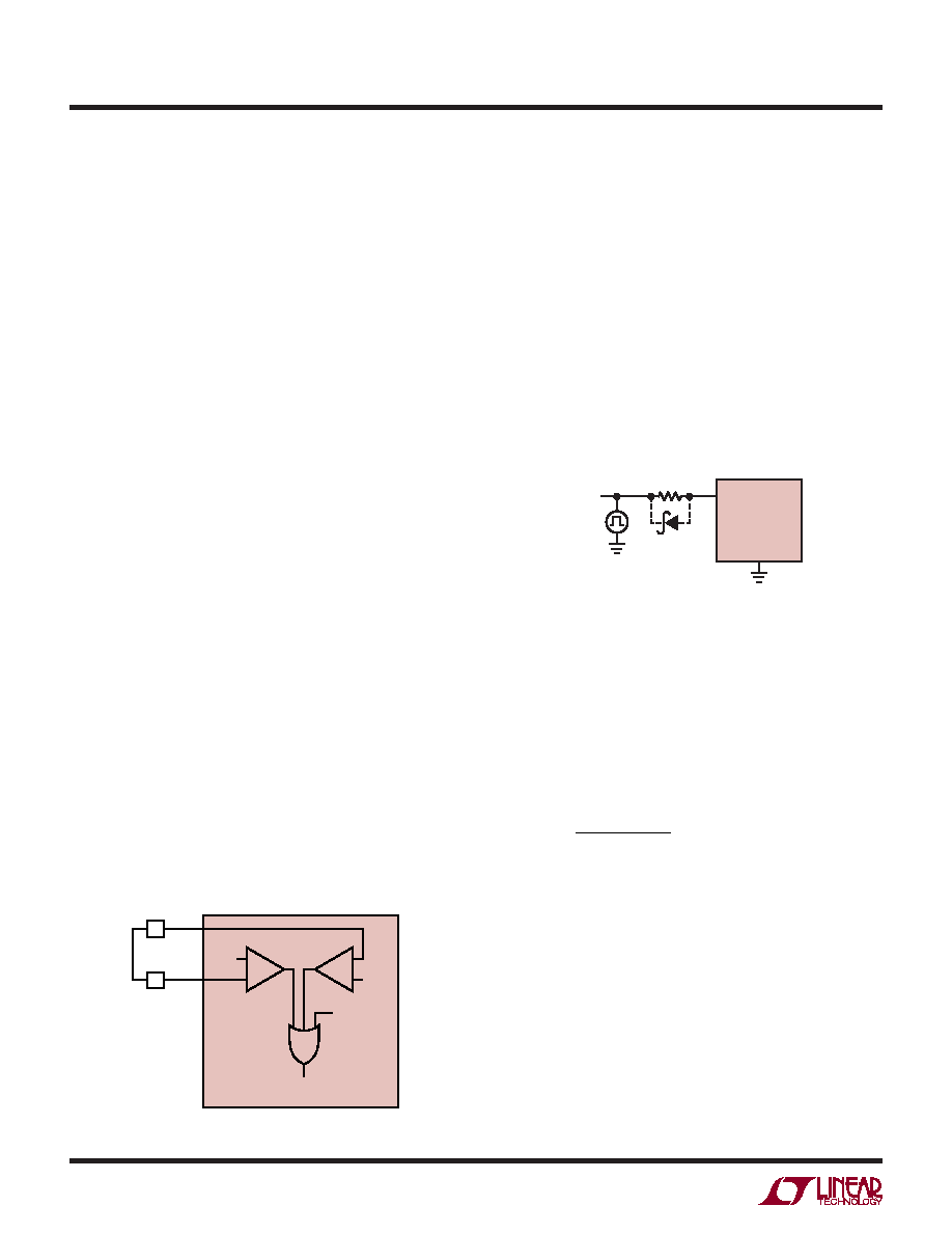
Referring to Figure 14, if the SHDN pin is connected to
VIN, then the overvoltage lockout threshold is set to the
typical maximum value of 38V.
Additionally, an internal comparator will force both chan-
nels into shutdown below the minimum VIN1 of 2.8V.
This feature can be used to prevent excessive discharge
of battery-operated systems. In addition to the VIN1 un-
dervoltage lockout, both channels will be disabled when
SHDN1 is less than 1.3V.
Programmable UVLO may be implemented using an input
voltage divider and one of the internal comparators (see
the Typical Applications section).
When the SHDN pin is taken above 1.3V, its respective
channel is allowed to operate. When the SHDN pin is
driven below 1.3V, its channel is placed in a low quiescent
current state. There is no hysteresis on the SHDN pins. If
the SHDN pins are not connected to VIN, then an internal
clamp regulates the SHDN pin voltage to 2.5V.
If the SHDN pin is driven by a logic signal greater than
2.5V, a series resistor is required to limit the current into
the SHDN pin to no more than 10A.
Referring to Figure 15, a 249k resistor will suffice for
a typical logic-level signal. If the logic signal is 5V or
greater, choose a current limiting resistor equal to RSHDN=
(VLOGIC – 2.5V)/10A. Place a small Schottky diode (such
as a BAT54) in parallel to the current-limiting resistor as
shown in Figure 15.
KeeptheconnectionsfromanyseriesresistorstotheSHDN
pins short and make sure that the interplane or surface
capacitance to switching nodes is minimized.
Figure 14. Connect SHDN to VIN to Select Default OVLO and UVLO
Figure 15. External Control of the SHDN Pin
+
–
+
–
1.3V
38V
THERMAL
SHUTDOWN
SHDN1
VINX
LT3692
3692 F15
CHANNEL
DISABLE
LT3692
3692 F15
SHDN
RSHDN
+
–
SCHOTTKY
OPTIONAL
IF VLOGIC < 5V
VLOGIC
Soft-Start
The output of the LT3692 regulates to the lowest voltage
presentateithertheSSpinoraninternal0.806Vreference.
A capacitor from the SS pin to ground is charged by an
internal 12A current source resulting in a linear output
ramp from 0V to the regulated output whose duration is
given by:
tRAMP =
CSS 0.806V
12A
At power-up, a reset signal sets the soft-start latch and
discharges both SS pins to approximately 0V to ensure
proper start-up. When both SS pins are fully discharged
the latch is reset and the internal 12A current source
starts to charge the SS pin.
When the SS pin voltage is below 115mV, the VC pin is
pulled low which disables switching. This allows the SS
pin to be used as an individual shutdown for each channel.
As the SS pin voltage rises above 90mV, the VC pin is re-
leased and the output is regulated to the SS voltage. When
the SS pin voltage exceeds the internal 0.806V reference,
相關(guān)PDF資料 |
PDF描述 |
|---|---|
| LT3692EUH#PBF | 5.8 A DUAL SWITCHING CONTROLLER, 2750 kHz SWITCHING FREQ-MAX, PQCC32 |
| LT3724MPFE#TR | SWITCHING CONTROLLER, 225 kHz SWITCHING FREQ-MAX, PDSO16 |
| LT3740EDHC | 0.14 A SWITCHING CONTROLLER, 330 kHz SWITCHING FREQ-MAX, PDSO16 |
| LT3741EFE#PBF | SWITCHING CONTROLLER, 1070 kHz SWITCHING FREQ-MAX, PDSO20 |
| LT3741IFE#TRPBF | SWITCHING CONTROLLER, 1070 kHz SWITCHING FREQ-MAX, PDSO20 |
相關(guān)代理商/技術(shù)參數(shù) |
參數(shù)描述 |
|---|---|
| LT3693 | 制造商:LINER 制造商全稱:Linear Technology 功能描述:Monolithic Dual Tracking |
| LT36931DD#PBF | 制造商:Linear Technology 功能描述: |
| LT3693EDD#PBF | 功能描述:IC REG BUCK ADJ 3.5A 10DFN RoHS:是 類別:集成電路 (IC) >> PMIC - 穩(wěn)壓器 - DC DC 開關(guān)穩(wěn)壓器 系列:- 標(biāo)準(zhǔn)包裝:250 系列:- 類型:降壓(降壓) 輸出類型:固定 輸出數(shù):1 輸出電壓:1.2V 輸入電壓:2.05 V ~ 6 V PWM 型:電壓模式 頻率 - 開關(guān):2MHz 電流 - 輸出:500mA 同步整流器:是 工作溫度:-40°C ~ 85°C 安裝類型:表面貼裝 封裝/外殼:6-UFDFN 包裝:帶卷 (TR) 供應(yīng)商設(shè)備封裝:6-SON(1.45x1) 產(chǎn)品目錄頁面:1032 (CN2011-ZH PDF) 其它名稱:296-25628-2 |
| LT3693EDD#TRPBF | 功能描述:IC REG BUCK ADJ 3.5A 10DFN RoHS:是 類別:集成電路 (IC) >> PMIC - 穩(wěn)壓器 - DC DC 開關(guān)穩(wěn)壓器 系列:- 設(shè)計資源:Design Support Tool 標(biāo)準(zhǔn)包裝:1 系列:- 類型:升壓(升壓) 輸出類型:固定 輸出數(shù):1 輸出電壓:3V 輸入電壓:0.75 V ~ 2 V PWM 型:- 頻率 - 開關(guān):- 電流 - 輸出:100mA 同步整流器:是 工作溫度:-40°C ~ 85°C 安裝類型:表面貼裝 封裝/外殼:SOT-23-5 細(xì)型,TSOT-23-5 包裝:剪切帶 (CT) 供應(yīng)商設(shè)備封裝:TSOT-23-5 其它名稱:AS1323-BTTT-30CT |
| LT3693EDDPBF | 制造商:Linear Technology 功能描述:DC-DC Converter Step-Down 3.6-36V DFN10 |
發(fā)布緊急采購,3分鐘左右您將得到回復(fù)。