- 您現(xiàn)在的位置:買賣IC網(wǎng) > PDF目錄44968 > LSM2-T/6-D12G-C (CD TECHNOLOGIES INC) 1-OUTPUT 19.8 W DC-DC REG PWR SUPPLY MODULE PDF資料下載
參數(shù)資料
| 型號(hào): | LSM2-T/6-D12G-C |
| 廠商: | CD TECHNOLOGIES INC |
| 元件分類: | 電源模塊 |
| 英文描述: | 1-OUTPUT 19.8 W DC-DC REG PWR SUPPLY MODULE |
| 封裝: | ROHS COMPLIANT PACKAGE-7 |
| 文件頁數(shù): | 7/17頁 |
| 文件大小: | 1504K |
| 代理商: | LSM2-T/6-D12G-C |
[8] If one converter is slaving to another master converter, there will be a very
short phase lag between the two converters. This can usually be ignored.
[9] You may connect two or more Sequence inputs in parallel from two con-
verters. Be aware of the increasing pull-up bias current and reduced input
impedance.
[10] Any external capacitance added to the converter’s output may affect ramp
up/down times and ramp tracking accuracy.
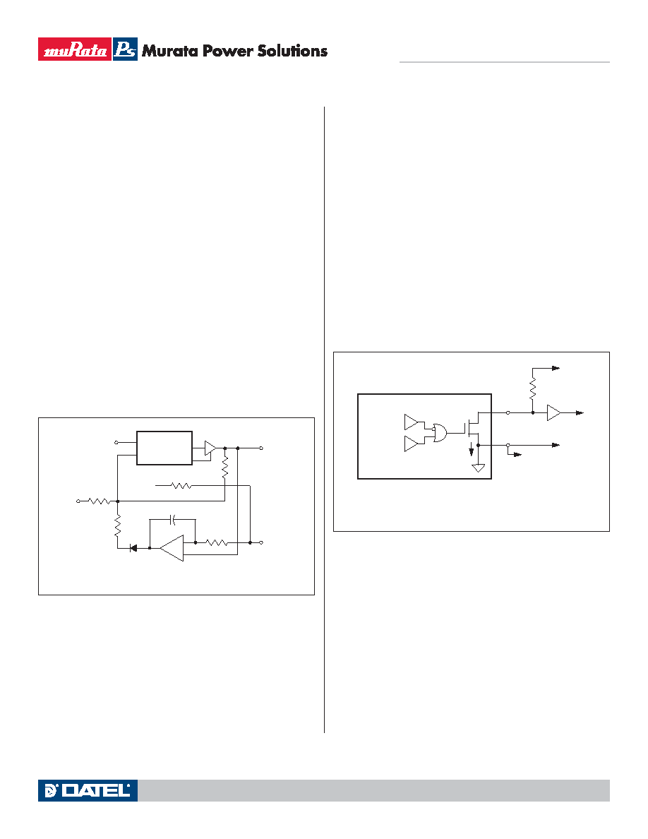
Power Good Output
The Power Good Output consists of an unterminated BSS138 small signal
field effect transistor and a dual window comparator input circuit driving the
gate of the FET. Power Good is TRUE (open drain, high impedance state) if the
converter’s power output voltage is within about ±10% of the setpoint. Thus,
the PG TRUE condition indicates that the converter is approximately within
regulation. Since an overcurrent condition occurs at about 2% output voltage
reduction, the Power Good does not directly measure an output overcurrent
condition at rated maximum output current. However, gross overcurrent or an
output short circuit will set Power Good to FALSE (+0.2V saturation, low imped-
ance condition).
Figure 18. Equivalent Power Good Circuit
Using a simple connection to external logic (and returned to the converter’s
Common connection), the Power Good output is unterminated so that the user
may adapt the output to a variety of logic families. The PG pin may therefore
be used with logic voltages which are not necessarily the same as the input
or output power voltages. Install an external pullup resistor to the logic supply
voltage which is compatible with your logic system. When the Power Good is
out of limit, the FET is at saturation, approximately +0.2V output. Keep this
LOW (FALSE) pulldown current to less than 10mA.
Please note that Power Good is briefly false during Sequence ramp-up.
Ignore Power Good while in transition.
MDC_LSM2 Series.B01 Page 15 of 17
Technical enquiries email: sales@murata-ps.com, tel: +1 508 339 3000
www.murata-ps.com
LSM2 Series
Single Putput, Non-Isolated
Selectable-Output POL DC/DC Converters
Guidelines for Sequence/Track Applications
[1] Leave the converter’s On/Off Enable control (if installed) in the On setting.
Normally, you should just leave the On/Off pin open.
[2] Allow the converter to stabilize (typically less than 20 mS after +VIN power
on) before raising the Sequence input. Also, if you wish to have a ramped
power down, leave +VIN powered all during the down ramp. Do not simply
shut off power.
[3] If you do not use the Sequence/Track pin, leave it open or tied to +VIN.
[4] Observe the Output slew rate relative to the Sequence input. A rough
guide is 2 Volts per millisecond maximum slew rate. If you exceed this
slew rate on the Sequence pin, the converter will simply ramp up at
it’s maximum output slew rate (and will not necessarily track the faster
Sequence input). The reason to carefully consider the slew rate limitation
is in case you want two different POL’s to precisely track each other.
[5] Be aware of the input characteristics of the Sequence pin. The high input
impedance affects the time constant of any small external ramp capacitor.
And the bias current will slowly charge up any external caps over time
if they are not grounded. The internal pull-up resistor to +VIN is typically
400k
W to 1MW.
Notice in the simplified Sequence/Track equivalent circuit (Figure 17) that
a blocking diode effectively disconnects this circuit when the Sequence/
Track pin is pulled up to +VIN or left open.
Figure 17. Sequence/Track Simplified Equivalent Schematic
[6] Allow the converter to eventually achieve its full-rated setpoint output
voltage. Do not remain in ramp up/down mode indefinitely. The converter
is characterized and meets all its specifications only at the setpoint volt-
age (plus or minus any trim voltage). During the ramp-up phase, the con-
verter is not considered fully in regulation. This may affect performance
with excessive high current loads at turn-on.
[7] The Sequence is a sensitive input into the feedback control loop of the
converter. Avoid noise and long leads on this input. Keep all wiring very
short. Use shielding if necessary. Consider adding a small parallel ceramic
capacitor across the Sequence/Track input (see Figure 16) to block any
external high frequency noise.
相關(guān)PDF資料 |
PDF描述 |
|---|---|
| LSM2-T/6-D12-C | 1-OUTPUT 19.8 W DC-DC REG PWR SUPPLY MODULE |
| LSM2-T/10-W3NG-C | 1-OUTPUT 33 W DC-DC REG PWR SUPPLY MODULE |
| LSM2-T/6-D12N-C | 1-OUTPUT 19.8 W DC-DC REG PWR SUPPLY MODULE |
| LSM2-T/16-W3-C | 1-OUTPUT 52.8 W DC-DC REG PWR SUPPLY MODULE |
| LSM2-T/16-D12N-C | 1-OUTPUT 52.8 W DC-DC REG PWR SUPPLY MODULE |
相關(guān)代理商/技術(shù)參數(shù) |
參數(shù)描述 |
|---|---|
| LSM2T6W3C | 制造商:MURATA 功能描述:Pb Free |
| LSM2U | 功能描述:限位開關(guān) LIMIT SWITCH RoHS:否 制造商:Honeywell 觸點(diǎn)形式:SPDT 執(zhí)行器:Non-Contact 電流額定值:30 mA 電壓額定值 AC: 電壓額定值 DC:3.6 V 工作力:10 g IP 等級(jí):IP 67 NEMA 額定值:1, 4, 12, 13 端接類型:4-Pin M12 Connector 安裝:SMD/SMT |
| LSM-3.3/10-D12 | 功能描述:DC/DC轉(zhuǎn)換器 33W 12V to 3.3V 10A SMT Package RoHS:否 制造商:Murata 產(chǎn)品: 輸出功率: 輸入電壓范圍:3.6 V to 5.5 V 輸入電壓(標(biāo)稱): 輸出端數(shù)量:1 輸出電壓(通道 1):3.3 V 輸出電流(通道 1):600 mA 輸出電壓(通道 2): 輸出電流(通道 2): 安裝風(fēng)格:SMD/SMT 封裝 / 箱體尺寸: |
| LSM-3.3/10-D12-C | 功能描述:DC/DC轉(zhuǎn)換器 33W 12V to 3.3V 10A RoHS:否 制造商:Murata 產(chǎn)品: 輸出功率: 輸入電壓范圍:3.6 V to 5.5 V 輸入電壓(標(biāo)稱): 輸出端數(shù)量:1 輸出電壓(通道 1):3.3 V 輸出電流(通道 1):600 mA 輸出電壓(通道 2): 輸出電流(通道 2): 安裝風(fēng)格:SMD/SMT 封裝 / 箱體尺寸: |
| LSM-3.3/10-D12EB | 制造商:MURATA 制造商全稱:Murata Manufacturing Co., Ltd. 功能描述:10 Amp DC/DC Power Converter Evaluation Boards |
發(fā)布緊急采購,3分鐘左右您將得到回復(fù)。