- 您現(xiàn)在的位置:買賣IC網(wǎng) > PDF目錄44968 > LSM2-T/6-D12G-C (CD TECHNOLOGIES INC) 1-OUTPUT 19.8 W DC-DC REG PWR SUPPLY MODULE PDF資料下載
參數(shù)資料
| 型號: | LSM2-T/6-D12G-C |
| 廠商: | CD TECHNOLOGIES INC |
| 元件分類: | 電源模塊 |
| 英文描述: | 1-OUTPUT 19.8 W DC-DC REG PWR SUPPLY MODULE |
| 封裝: | ROHS COMPLIANT PACKAGE-7 |
| 文件頁數(shù): | 6/17頁 |
| 文件大?。?/td> | 1504K |
| 代理商: | LSM2-T/6-D12G-C |
MDC_LSM2 Series.B01 Page 14 of 17
Technical enquiries email: sales@murata-ps.com, tel: +1 508 339 3000
www.murata-ps.com
LSM2 Series
Single Putput, Non-Isolated
Selectable-Output POL DC/DC Converters
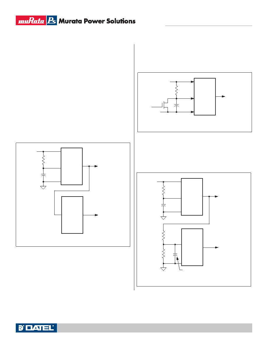
Figure 15. Self-Ramping Power Up
Operation
To use the Sequence pin after power start-up stabilizes, apply a rising external
voltage to the Sequence input. As the voltage rises, the output voltage will
track the Sequence input (gain = 1). The output voltage will stop rising when it
reaches the normal set point for the converter. The Sequence input may option-
ally continue to rise without any effect on the output. Keep the Sequence input
voltage below the converter’s input supply voltage.
Use a similar strategy on power down. The output voltage will stay constant
until the Sequence input falls below the set point.
Any strategy may be used to deliver the power up/down ramps. The circuits
below show simple RC networks but you may also use operational amplifiers,
D/A converters, etc.
Circuits
The circuits shown in Figures 14 through 16 introduce several concepts when
using these Sequencing controls on Point-of-Load (POL) converters. These
circuits are only for reference and are not intended as final designs ready for
your application. Also, numerous connections are omitted for clarity.
Figure 15 shows a single POL and the same RC network. However, we have
added a FET at Q1 as an up/down control. When VIN power is applied to the
POL, Q1 is biased on, shorting out the Sequence pin. When Q1’s gate is biased
off, R1 charges C1 and the POL’s output ramps up at the R1-C1 slew rate. Note:
Q1’s gate would typically be controlled from some external digital logic.
Figure 14. Wiring for Simultaneous Phasing
Figure 16. Proportional Phasing
Figure 14 shows a basic Master (POL A) and Slave (POL B) connected so the
POL B ramps up identically to POL A as shown in timing diagram, Figure 10. RC
network R1 and C1 charge up at a rate set by the R1-C1 time constant, giving
a roughly linear ramp. As POL A reaches 3.3VOUT (the setpoint of POL B), POL
B will stop rising. POL A then continues rising until it reaches 5V. R1 should be
significantly smaller than the internal bias current resistor from the Sequence
pin. Start with a 20k
W value. We assume that the critical phase is only on
power up therefore there is no provision for ramped power down.
If you wish to have a ramped power down (rather than a step down), add a
small resistor in series with Q1’s drain.
Figure 16 shows both a RC ramp on Master POL A and a proportional track-
ing divider (R2 and R3) on POL B. We have also added an optional very small
noise filter cap at C2. Figure 16’s circuit corresponds roughly to Figure 11’s
timing for power up.
相關(guān)PDF資料 |
PDF描述 |
|---|---|
| LSM2-T/6-D12-C | 1-OUTPUT 19.8 W DC-DC REG PWR SUPPLY MODULE |
| LSM2-T/10-W3NG-C | 1-OUTPUT 33 W DC-DC REG PWR SUPPLY MODULE |
| LSM2-T/6-D12N-C | 1-OUTPUT 19.8 W DC-DC REG PWR SUPPLY MODULE |
| LSM2-T/16-W3-C | 1-OUTPUT 52.8 W DC-DC REG PWR SUPPLY MODULE |
| LSM2-T/16-D12N-C | 1-OUTPUT 52.8 W DC-DC REG PWR SUPPLY MODULE |
相關(guān)代理商/技術(shù)參數(shù) |
參數(shù)描述 |
|---|---|
| LSM2T6W3C | 制造商:MURATA 功能描述:Pb Free |
| LSM2U | 功能描述:限位開關(guān) LIMIT SWITCH RoHS:否 制造商:Honeywell 觸點形式:SPDT 執(zhí)行器:Non-Contact 電流額定值:30 mA 電壓額定值 AC: 電壓額定值 DC:3.6 V 工作力:10 g IP 等級:IP 67 NEMA 額定值:1, 4, 12, 13 端接類型:4-Pin M12 Connector 安裝:SMD/SMT |
| LSM-3.3/10-D12 | 功能描述:DC/DC轉(zhuǎn)換器 33W 12V to 3.3V 10A SMT Package RoHS:否 制造商:Murata 產(chǎn)品: 輸出功率: 輸入電壓范圍:3.6 V to 5.5 V 輸入電壓(標稱): 輸出端數(shù)量:1 輸出電壓(通道 1):3.3 V 輸出電流(通道 1):600 mA 輸出電壓(通道 2): 輸出電流(通道 2): 安裝風(fēng)格:SMD/SMT 封裝 / 箱體尺寸: |
| LSM-3.3/10-D12-C | 功能描述:DC/DC轉(zhuǎn)換器 33W 12V to 3.3V 10A RoHS:否 制造商:Murata 產(chǎn)品: 輸出功率: 輸入電壓范圍:3.6 V to 5.5 V 輸入電壓(標稱): 輸出端數(shù)量:1 輸出電壓(通道 1):3.3 V 輸出電流(通道 1):600 mA 輸出電壓(通道 2): 輸出電流(通道 2): 安裝風(fēng)格:SMD/SMT 封裝 / 箱體尺寸: |
| LSM-3.3/10-D12EB | 制造商:MURATA 制造商全稱:Murata Manufacturing Co., Ltd. 功能描述:10 Amp DC/DC Power Converter Evaluation Boards |
發(fā)布緊急采購,3分鐘左右您將得到回復(fù)。