- 您現(xiàn)在的位置:買賣IC網(wǎng) > PDF目錄358934 > LPC47N227MN Peripheral IC PDF資料下載
參數(shù)資料
| 型號(hào): | LPC47N227MN |
| 英文描述: | Peripheral IC |
| 中文描述: | 外圍芯片 |
| 文件頁數(shù): | 196/228頁 |
| 文件大?。?/td> | 1269K |
| 代理商: | LPC47N227MN |
第1頁第2頁第3頁第4頁第5頁第6頁第7頁第8頁第9頁第10頁第11頁第12頁第13頁第14頁第15頁第16頁第17頁第18頁第19頁第20頁第21頁第22頁第23頁第24頁第25頁第26頁第27頁第28頁第29頁第30頁第31頁第32頁第33頁第34頁第35頁第36頁第37頁第38頁第39頁第40頁第41頁第42頁第43頁第44頁第45頁第46頁第47頁第48頁第49頁第50頁第51頁第52頁第53頁第54頁第55頁第56頁第57頁第58頁第59頁第60頁第61頁第62頁第63頁第64頁第65頁第66頁第67頁第68頁第69頁第70頁第71頁第72頁第73頁第74頁第75頁第76頁第77頁第78頁第79頁第80頁第81頁第82頁第83頁第84頁第85頁第86頁第87頁第88頁第89頁第90頁第91頁第92頁第93頁第94頁第95頁第96頁第97頁第98頁第99頁第100頁第101頁第102頁第103頁第104頁第105頁第106頁第107頁第108頁第109頁第110頁第111頁第112頁第113頁第114頁第115頁第116頁第117頁第118頁第119頁第120頁第121頁第122頁第123頁第124頁第125頁第126頁第127頁第128頁第129頁第130頁第131頁第132頁第133頁第134頁第135頁第136頁第137頁第138頁第139頁第140頁第141頁第142頁第143頁第144頁第145頁第146頁第147頁第148頁第149頁第150頁第151頁第152頁第153頁第154頁第155頁第156頁第157頁第158頁第159頁第160頁第161頁第162頁第163頁第164頁第165頁第166頁第167頁第168頁第169頁第170頁第171頁第172頁第173頁第174頁第175頁第176頁第177頁第178頁第179頁第180頁第181頁第182頁第183頁第184頁第185頁第186頁第187頁第188頁第189頁第190頁第191頁第192頁第193頁第194頁第195頁當(dāng)前第196頁第197頁第198頁第199頁第200頁第201頁第202頁第203頁第204頁第205頁第206頁第207頁第208頁第209頁第210頁第211頁第212頁第213頁第214頁第215頁第216頁第217頁第218頁第219頁第220頁第221頁第222頁第223頁第224頁第225頁第226頁第227頁第228頁
SMSC DS – LPC47M192
Page 196
Rev. 03/30/05
DATASHEET
HARDWARE MONITORING BLOCK
(T
A
= 0
o
C – 70
o
C, HV
CC
= +3.3 ± 10%)
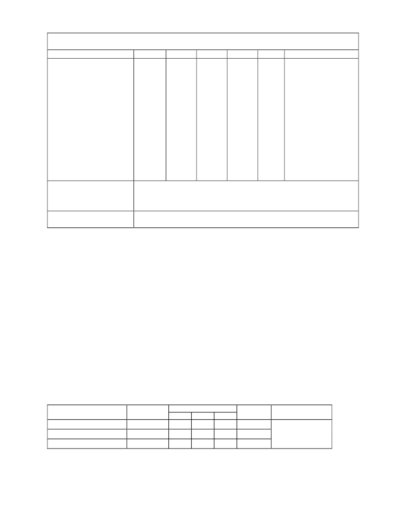
PARAMETER
Temperature-to-Digital
Converter Characteristics
Internal Temperature Accuracy
External
Diode
Accuracy
Remote Source Current
High Level
Low Level
SYMBOL
MIN
-3
-2
-5
-3
TYP
±1
±1
90
5.5
MAX
+3
+2
+5
+3
130
7.5
UNITS
o
C
o
C
o
C
o
C
o
C
o
C
μA
μA
COMMENTS
Sensor
0
0
C <= T
A
<= 70
0
C
40
0
C <= T
A
<= 70
0
C
Resolution
-40
0
C <= T
S
<= 125
0
C
40
0
C <= T
S
<= 100
0
C
Resolution
I
ANG
Type Buffer – Analog
Inputs
(Dx+,
Dx-,
+3.3V_IN, +5V_IN, +12V_IN)
V
CC
Supply Current Active
+2.5V_IN,
Refer to “Appendix A – Thermal Diode Parameters” and “Appendix B – ADC
Voltage Conversion”.
See “Supply Current” subsection in “Hardware Monitoring Block Specifications”
section above.
Notes
:
Voltages are measured from the local ground potential, unless otherwise specified.
Typicals are at TA=25°C and represent most likely parametric norm.
The maximum allowable power dissipation at any temperature is PD = (TJmax - TA) / QJA.
Timing specifications are tested at the TTL logic levels, VIL=0.4V for a falling edge and VIH=2.4V for a rising
edge. TRI-STATE output voltage is forced to 1.4V.
Note 1:
All leakage currents are measured with all pins in high impedance.
Note 2:
The minimum value given for V
TR
applies when V
CC
is active. When V
CC
is 0V, the minimum V
TR
is 0V.
Note 3:
Max I
TRI
with V
CC
= 3.3V (nominal) is 5mA
Max I
TRI
with V
CC
= 0V (nomial) is 250uA
Note 4:
TUE (Total Unadjusted Error) includes Offset, Gain and Linearity errors of the ADC.
Note 5:
Total Monitoring Cycle Time includes all temperature conversions, all analog input voltage conversions.
Note 6:
The cycle time for option 1 is 542.336ms (typical) if 128 measurements are averaged for the remote diode
temperature reading and 8 measurements are averaged for all voltage and the internal temperature reading. It is
67.792ms (typical) for option 2 if 16 measurements are averaged for the remote diode temperature reading and a
single measurement is taken for all voltage and the internal temperature reading (i.e., no averaging).
Note 7:
V
OH
min and I
OH
does not apply to the RESET# and THERM# open-drain functions.
11.3.1 CAPACITANCE VALUES FOR PINS
The input and output capacitance applies to both the Super I/O Block and the Hardware Monitoring Block digital pins.
CAPACITANCE T
A
= 25
o
C; fc = 1MHz; V
CC
= 3.3V ±10%
PARAMETER
Clock Input Capacitance
LIMITS
TYP
SYMBOL
C
IN
C
IN
C
OUT
MIN
MAX
20
UNIT
pF
TEST CONDITION
All pins except pin
under test tied to AC
ground
Input Capacitance
10
pF
Output Capacitance
Note:
The input capacitance of a port is measured at the connector pins.
20
pF
相關(guān)PDF資料 |
PDF描述 |
|---|---|
| LPC47M10X | Microcontroller |
| LPC47M182 | Microprocessor Crystal; Frequency:19.6608MHz; Frequency Tolerance:20ppm; Load Capacitance:18pF; Crystal Terminals:Radial Leaded; ESR:25ohm; Leaded Process Compatible:Yes; Mounting Type:Through Hole; No. of Pins:2 RoHS Compliant: Yes |
| LPC47N350 | LEGACY FREE KEYBOARD EMBEDDED CONTROLLER WITH SPI AND LPC DOCKING INTERFACE |
| LPC47N217 | 64 - PIN SUPUR I/O WITH LPC INTERFACE |
| LPC47N217-JN | 64 - PIN SUPUR I/O WITH LPC INTERFACE |
相關(guān)代理商/技術(shù)參數(shù) |
參數(shù)描述 |
|---|---|
| LPC47N227-MN | 制造商:Rochester Electronics LLC 功能描述:- Bulk |
| LPC47N227-MT | 功能描述:輸入/輸出控制器接口集成電路 Notebk I/O Contrllr RoHS:否 制造商:Silicon Labs 產(chǎn)品: 輸入/輸出端數(shù)量: 工作電源電壓: 最大工作溫度:+ 85 C 最小工作溫度:- 40 C 安裝風(fēng)格:SMD/SMT 封裝 / 箱體:QFN-64 封裝:Tray |
| LPC47N227-MV | 功能描述:輸入/輸出控制器接口集成電路 100-Pin Mobile I/O RoHS:否 制造商:Silicon Labs 產(chǎn)品: 輸入/輸出端數(shù)量: 工作電源電壓: 最大工作溫度:+ 85 C 最小工作溫度:- 40 C 安裝風(fēng)格:SMD/SMT 封裝 / 箱體:QFN-64 封裝:Tray |
| LPC47N227TQFP | 制造商:Microchip Technology 功能描述:I/O Controller 制造商:Rochester Electronics LLC 功能描述:NOTEBOOK I/O CONTROLLER W/ LPC INTERFACE (TQFP PACKAGE) - Bulk |
| LPC47N237 | 制造商:SMSC 制造商全稱:SMSC 功能描述:3.3v I/O Controller for Port Replicators and Docking Stations |
發(fā)布緊急采購,3分鐘左右您將得到回復(fù)。