- 您現(xiàn)在的位置:買賣IC網(wǎng) > PDF目錄358934 > LPC47M14A-NC (SMSC Corporation) 128 PIN ENGANCED SUPER I/O CONTROLLER WITH AN LPC INTERFACE AND USB HUB PDF資料下載
參數(shù)資料
| 型號: | LPC47M14A-NC |
| 廠商: | SMSC Corporation |
| 英文描述: | 128 PIN ENGANCED SUPER I/O CONTROLLER WITH AN LPC INTERFACE AND USB HUB |
| 中文描述: | 128引腳ENGANCED超級I / O與LPC接口和USB集線器控制器 |
| 文件頁數(shù): | 162/205頁 |
| 文件大小: | 1219K |
| 代理商: | LPC47M14A-NC |
第1頁第2頁第3頁第4頁第5頁第6頁第7頁第8頁第9頁第10頁第11頁第12頁第13頁第14頁第15頁第16頁第17頁第18頁第19頁第20頁第21頁第22頁第23頁第24頁第25頁第26頁第27頁第28頁第29頁第30頁第31頁第32頁第33頁第34頁第35頁第36頁第37頁第38頁第39頁第40頁第41頁第42頁第43頁第44頁第45頁第46頁第47頁第48頁第49頁第50頁第51頁第52頁第53頁第54頁第55頁第56頁第57頁第58頁第59頁第60頁第61頁第62頁第63頁第64頁第65頁第66頁第67頁第68頁第69頁第70頁第71頁第72頁第73頁第74頁第75頁第76頁第77頁第78頁第79頁第80頁第81頁第82頁第83頁第84頁第85頁第86頁第87頁第88頁第89頁第90頁第91頁第92頁第93頁第94頁第95頁第96頁第97頁第98頁第99頁第100頁第101頁第102頁第103頁第104頁第105頁第106頁第107頁第108頁第109頁第110頁第111頁第112頁第113頁第114頁第115頁第116頁第117頁第118頁第119頁第120頁第121頁第122頁第123頁第124頁第125頁第126頁第127頁第128頁第129頁第130頁第131頁第132頁第133頁第134頁第135頁第136頁第137頁第138頁第139頁第140頁第141頁第142頁第143頁第144頁第145頁第146頁第147頁第148頁第149頁第150頁第151頁第152頁第153頁第154頁第155頁第156頁第157頁第158頁第159頁第160頁第161頁當(dāng)前第162頁第163頁第164頁第165頁第166頁第167頁第168頁第169頁第170頁第171頁第172頁第173頁第174頁第175頁第176頁第177頁第178頁第179頁第180頁第181頁第182頁第183頁第184頁第185頁第186頁第187頁第188頁第189頁第190頁第191頁第192頁第193頁第194頁第195頁第196頁第197頁第198頁第199頁第200頁第201頁第202頁第203頁第204頁第205頁
SMSC DS – LPC47M14X
Page 162
Rev. 03/19/2001
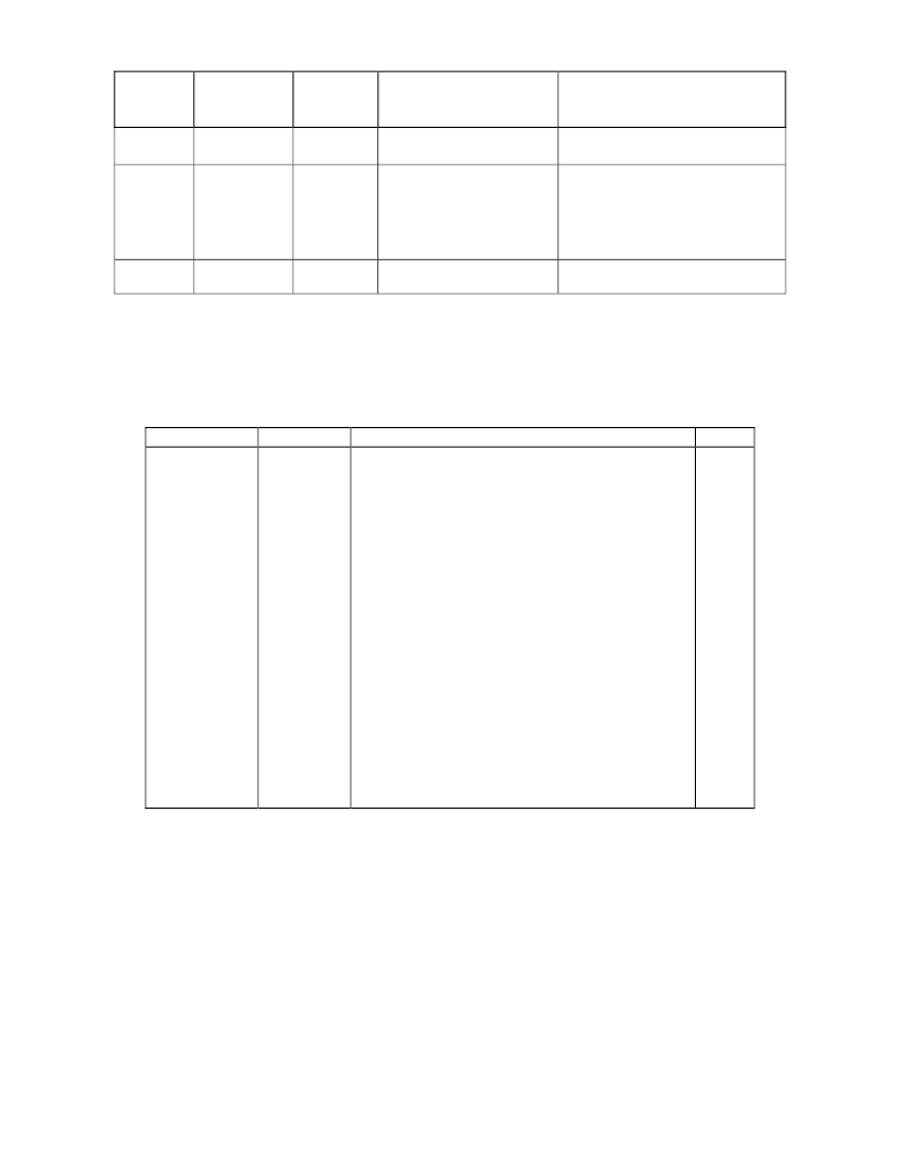
Table 65 – I/O Base Address Configuration Register Description
REGISTER
INDEX
(NOTE 1)
MPU-401
0x60,0x61
[0x0100:0x0FFE]
on 2-byte boundaries
Config. Port
0x26, 0x27
(Note 2)
On 2 byte boundaries
LOGICAL
DEVICE
NUMBER
0x0B
LOGICAL
DEVICE
BASE I/O
RANGE
FIXED
BASE OFFSETS
+0: MIDI DATA
+1: STATUS/COMMAND
See Configuration Register in Table
61. Accessed through the index and
DATA
ports
located
Configuration Port address and the
Configuration
Port
respectively.
n/a
Config.
Port
0x0100:0x0FFE
at
the
address
+1
0x0C
USB Hub
n/a
No Base I/O Address Range
allocated to the Hub Block
Note 1:
This chip uses address bits [A11:A0] to decode the base address of each of its logical devices. Bit 6 of the
OSC Global Configuration Register (CR24) must be set to ‘1’ and Address Bits [A15:A12] must be ‘0’ for 16 bit
address qualification.
Note 2:
The Configuration Port is at either 0x02E or 0x04E (for SYSOPT=0 or SYSOPT=1) at power up and can
replaced via the global configuration registers at 0x26 and 0x27.
be
Table 66 – Interrupt Select Configuration Register Description
NAME
REG INDEX
0x70 (R/W)
DEFINITION
STATE
C
Primary Interrupt
Select
Default=0x00 or
0x06
(Note 1)
on VCC POR,
VTR POR,
HARD RESET
and
SOFT RESET
Bits[3:0] selects which interrupt is used for the primary
Interrupt.
0x00= no interrupt selected
0x01= IRQ1
0x02= IRQ2/nSMI
0x03= IRQ3
0x04= IRQ4
0x05= IRQ5
0x06= IRQ6
0x07= IRQ7
0x08= IRQ8
0x09= IRQ9
0x0A= IRQ10
0x0B= IRQ11
0x0C= IRQ12
0x0D= IRQ13
0x0E= IRQ14
0x0F= IRQ15
Note:
All interrupts are edge high (except ECP/EPP)
Note:
nSMI is active low
Note
:
Note:
Note:
nSMI must be disabled to use IRQ2.
Note:
All IRQ’s are available in Serial IRQ mode.
Note 1:
The default value of the Primary Interrupt Select register for logical device 0 is 0x06.
An Interrupt is activated by setting the Interrupt Request Level Select 0 register to a non-zero value AND :
For the FDC logical device by setting DMAEN, bit D3 of the Digital Output Register.
For the PP logical device by setting IRQE, bit D4 of the Control Port and in addition
For the PP logical device in ECP mode by clearing serviceIntr, bit D2 of the ecr.
For the Serial Port logical device by setting any combination of bits D0-D3 in the IER
And by setting the OUT2 bit in the UART's Modem Control (MCR) Register.
For the KYBD by (refer to the KYBD controller section of this spec).
IRQs are disabled if not used/selected by any Logical Device. Refer to Note A.
相關(guān)PDF資料 |
PDF描述 |
|---|---|
| LPC47M14T-NC | 128 PIN ENGANCED SUPER I/O CONTROLLER WITH AN LPC INTERFACE AND USB HUB |
| LPC47M14S-NC | 128 PIN ENGANCED SUPER I/O CONTROLLER WITH AN LPC INTERFACE AND USB HUB |
| LPC47M192 | LPC SUPER I/O WITH HARDWARE MONITORING BLOCK |
| LPC47U32X | Peripheral (Multifunction) Controller |
| LPC47N227MN | Peripheral IC |
相關(guān)代理商/技術(shù)參數(shù) |
參數(shù)描述 |
|---|---|
| LPC47M14B-NC | 制造商:SMSC 制造商全稱:SMSC 功能描述:128 PIN ENGANCED SUPER I/O CONTROLLER WITH AN LPC INTERFACE AND USB HUB |
| LPC47M14C-NC | 制造商:SMSC 制造商全稱:SMSC 功能描述:128 PIN ENGANCED SUPER I/O CONTROLLER WITH AN LPC INTERFACE AND USB HUB |
| LPC47M14D-NC | 制造商:SMSC 制造商全稱:SMSC 功能描述:128 PIN ENGANCED SUPER I/O CONTROLLER WITH AN LPC INTERFACE AND USB HUB |
| LPC47M14E-NC | 制造商:SMSC 制造商全稱:SMSC 功能描述:128 PIN ENGANCED SUPER I/O CONTROLLER WITH AN LPC INTERFACE AND USB HUB |
| LPC47M14F-NC | 制造商:SMSC 制造商全稱:SMSC 功能描述:128 PIN ENGANCED SUPER I/O CONTROLLER WITH AN LPC INTERFACE AND USB HUB |
發(fā)布緊急采購,3分鐘左右您將得到回復(fù)。