- 您現(xiàn)在的位置:買賣IC網(wǎng) > PDF目錄299411 > LP3985IM5-285/NOPB (NATIONAL SEMICONDUCTOR CORP) 2.85 V FIXED POSITIVE LDO REGULATOR, 0.1 V DROPOUT, PDSO5 PDF資料下載
參數(shù)資料
| 型號(hào): | LP3985IM5-285/NOPB |
| 廠商: | NATIONAL SEMICONDUCTOR CORP |
| 元件分類: | 固定正電壓單路輸出LDO穩(wěn)壓器 |
| 英文描述: | 2.85 V FIXED POSITIVE LDO REGULATOR, 0.1 V DROPOUT, PDSO5 |
| 封裝: | SOT-23, SOP-5 |
| 文件頁數(shù): | 14/17頁 |
| 文件大?。?/td> | 993K |
| 代理商: | LP3985IM5-285/NOPB |
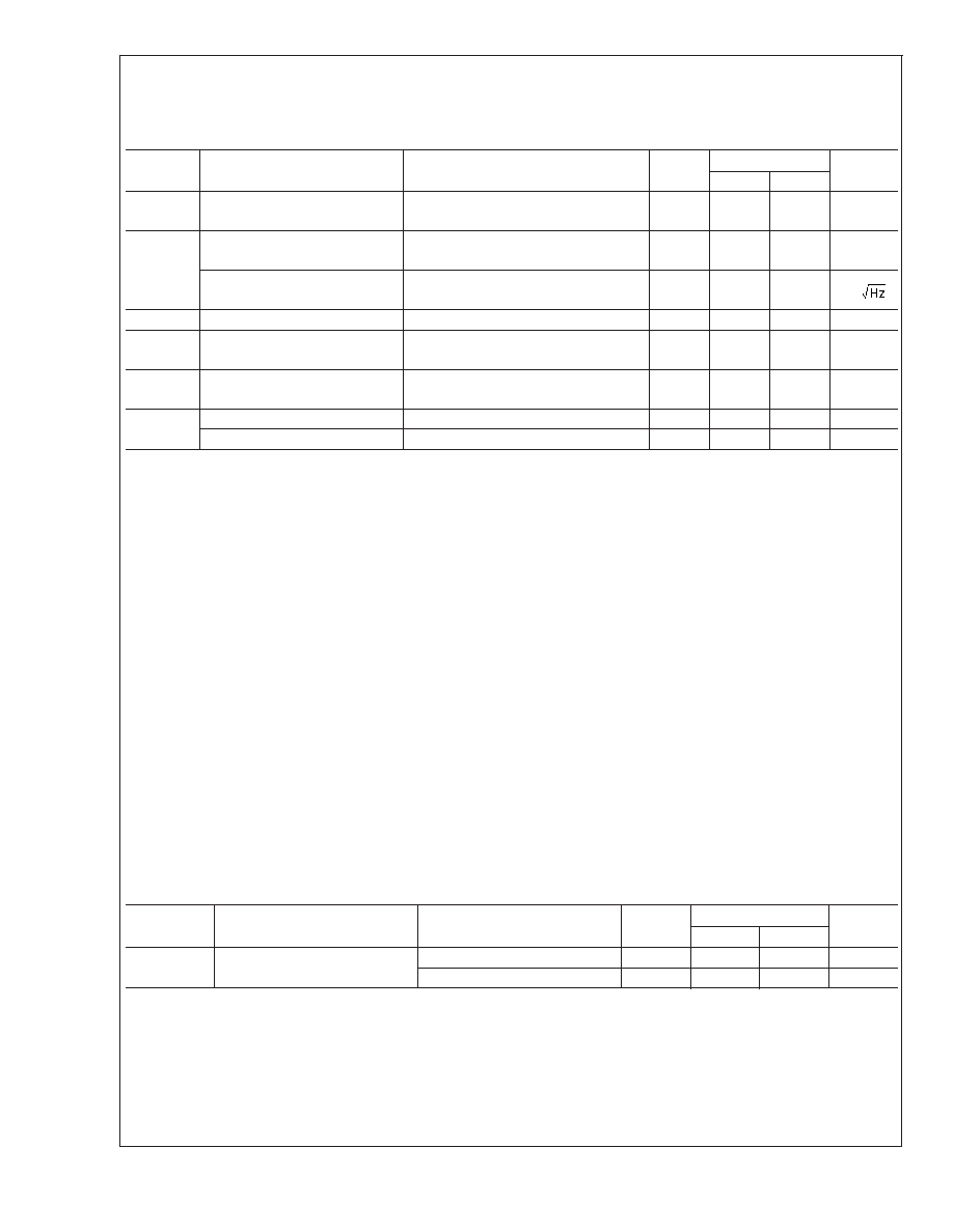
Electrical Characteristics (Continued)
Unless otherwise specified: V
IN =VOUT(nom) + 0.5V, CIN = 1 F, IOUT = 1mA, COUT = 1 F, CBYPASS = 0.01F. Typical values
and limits appearing in standard typeface are for T
J = 25C. Limits appearing in boldface type apply over the entire junction
temperature range for operation, 40C to +125C. (Note 7) (Note 8)
Symbol
Parameter
Conditions
Typ
Limit
Units
Min
Max
T
ON
Turn-On Time
C
BYPASS = 0.01 F
200
s
e
n
Output Noise Voltage(Note 12)
BW = 10 Hz to 100 kHz,
C
OUT = 1F
30
Vrms
Output Noise Density
C
BP = 0
230
nV/
I
EN
Maximum Input Current at EN
V
EN = 0.4 and VIN = 6.0
±1nA
V
IL
Maximum Low Level Input
Voltage at EN
V
IN = 2.5 to 6.0V
0.4
V
IH
Minimum High Level Input
Voltage at EN
V
IN = 2.5 to 6.0V
1.4
V
TSD
Thermal Shutdown Temperature
160
C
Thermal Shutdown Hysteresis
20
C
Note 1: Absolute Maximum Ratings are limits beyond which damage to the device may occur. Operating Ratings are conditions under which operation of the device
is guaranteed. Operating Ratings do not imply guaranteed performance limits. For guaranteed performance limits and associated test conditions, see the Electrical
Characteristics tables.
Note 2: All voltages are with respect to the potential at the GND pin.
Note 3: Additional information on lead temperature and pad temperature can be found in National Semiconductor Application Note (AN-1112).
Note 4: The Absolute Maximum power dissipation depends on the ambient temperature and can be calculated using the formula: PD =(TJ -TA)/θJA,
where TJ is the junction temperature, TA is the ambient temperature, and θ JA is the junction-to-ambient thermal resistance. The 364mW rating for SOT23-5
appearing under Absolute Maximum Ratings results from substituting the Absolute Maximum junction temperature, 150C, for TJ, 70C for TA, and 220C/W for θJA.
More power can be dissipated safely at ambient temperatures below 70C . Less power can be dissipated safely at ambient temperatures above 70C. The Absolute
Maximum power dissipation can be increased by 4.5mW for each degree below 70C, and it must be derated by 4.5mW for each degree above 70C.
Note 5: The human body model is 100pF discharged through 1.5k
resistor into each pin. The machine model is a 200 pF capacitor discharged directly into each
pin.
Note 6: Like the Absolute Maximum power dissipation, the maximum power dissipation for operation depends on the ambient temperature. The 250mW rating for
SOT23-5 appearing under Operating Ratings results from substituting the maximum junction temperature for operation, 125C, for TJ, 70C for TA, and 220C/W for
θJA into (Note 4) above. More power can be dissipated at ambient temperatures below 70C . Less power can be dissipated at ambient temperatures above 70C.
The maximum power dissipation for operation can be increased by 4.5mW for each degree below 70C, and it must be derated by 4.5mW for each degree above
70C.
Note 7: All limits are guaranteed. All electrical characteristics having room-temperature limits are tested during production with TJ = 25C or correlated using
Statistical Quality Control (SQC) methods. All hot and cold limits are guaranteed by correlating the electrical characteristics to process and temperature variations
and applying statistical process control.
Note 8: The target output voltage, which is labeled VOUT(nom), is the desired voltage option.
Note 9: An increase in the load current results in a slight decrease in the output voltage and vice versa.
Note 10: Dropout voltage is the input-to-output voltage difference at which the output voltage is 100mV below its nominal value. This specification does not apply
for input voltages below 2.5V.
Note 11: Turn-on time is time measured between the enable input just exceeding VIH and the output voltage just reaching 95% of its nominal value.
Note 12: The output noise varies with output voltage option. The 30Vrms is measured with 2.5V voltage option. To calculate an approximated output noise for other
options, use the equation: (30Vrms)(X)/2.5, where X is the voltage option value.
Recommended Output Capacitor
Symbol
Parameter
Conditions
Nominal
Value
Limit
Units
Min
Max
C
OUT
Output Capacitor
1.0
0.7
F
ESR
5
500
m
Note 13: The minimum value of capacitance for stability and correct operation is 0.7F. The Capacitor tolerance should be ± 30% or better over the temperature
range. The full range of operating conditions for the capacitor in the application should be considered during device selection to ensure this minimum capacitance
specification is met. The recommended capacitor type is X7R to meet the full device temperature spec of -40oCto125oC. See the capacitor section in Application
Hints.
LP3985
www.national.com
6
相關(guān)PDF資料 |
PDF描述 |
|---|---|
| LP3985IM5X-2.6/NOPB | 2.6 V FIXED POSITIVE LDO REGULATOR, 0.1 V DROPOUT, PDSO5 |
| LP3985IM5X-2.9/NOPB | 2.9 V FIXED POSITIVE LDO REGULATOR, 0.1 V DROPOUT, PDSO5 |
| LP3985IM5X-3.1/NOPB | 3.1 V FIXED POSITIVE LDO REGULATOR, 0.1 V DROPOUT, PDSO5 |
| LP3985IM5X-3.2/NOPB | 3.2 V FIXED POSITIVE LDO REGULATOR, 0.1 V DROPOUT, PDSO5 |
| LP61L1008AS-10 | 128K x 8 bit high speed 3.3V center power CMOS SRAM |
相關(guān)代理商/技術(shù)參數(shù) |
參數(shù)描述 |
|---|---|
| LP3985IM5-3.0 | 功能描述:低壓差穩(wěn)壓器 - LDO RoHS:否 制造商:Texas Instruments 最大輸入電壓:36 V 輸出電壓:1.4 V to 20.5 V 回動(dòng)電壓(最大值):307 mV 輸出電流:1 A 負(fù)載調(diào)節(jié):0.3 % 輸出端數(shù)量: 輸出類型:Fixed 最大工作溫度:+ 125 C 安裝風(fēng)格:SMD/SMT 封裝 / 箱體:VQFN-20 |
| LP3985IM5-3.0/NOPB | 功能描述:低壓差穩(wěn)壓器 - LDO 150Ma Low Noise CMOS LDO RoHS:否 制造商:Texas Instruments 最大輸入電壓:36 V 輸出電壓:1.4 V to 20.5 V 回動(dòng)電壓(最大值):307 mV 輸出電流:1 A 負(fù)載調(diào)節(jié):0.3 % 輸出端數(shù)量: 輸出類型:Fixed 最大工作溫度:+ 125 C 安裝風(fēng)格:SMD/SMT 封裝 / 箱體:VQFN-20 |
| LP3985IM5-3.0/NOPB | 制造商:Texas Instruments 功能描述:Linear Voltage Regulator IC |
| LP3985IM53.1 | 制造商:Texas Instruments 功能描述: |
| LP3985IM5-3.1 | 制造商:NATL SEMI 功能描述:3.1 V FIXED POSITIVE LDO REGULATOR, 0.1 V DROPOUT, PDSO5 制造商:Texas Instruments 功能描述:3.1 V FIXED POSITIVE LDO REGULATOR, 0.1 V DROPOUT, PDSO5 |
發(fā)布緊急采購,3分鐘左右您將得到回復(fù)。