- 您現(xiàn)在的位置:買賣IC網(wǎng) > PDF目錄384605 > LP39542RLX (NATIONAL SEMICONDUCTOR CORP) Zener Diode; Application: Low noise; Pd (mW): 250; Vz (V): 4.9 to 5.3; Condition Iz at Vz (mA): 0.5; C (pF) max: -; Condition VR at C (V):   ESD (kV) min: -; Package: LLD PDF資料下載
參數(shù)資料
| 型號: | LP39542RLX |
| 廠商: | NATIONAL SEMICONDUCTOR CORP |
| 元件分類: | 顯示驅(qū)動器 |
| 英文描述: | Zener Diode; Application: Low noise; Pd (mW): 250; Vz (V): 4.9 to 5.3; Condition Iz at Vz (mA): 0.5; C (pF) max: -; Condition VR at C (V):   ESD (kV) min: -; Package: LLD |
| 中文描述: | LED DISPLAY DRIVER, PBGA36 |
| 封裝: | 3 X 3 MM, 0.65 MM HEIGHT, 0.50 MM PITCH, MICRO, SMD-36 |
| 文件頁數(shù): | 32/58頁 |
| 文件大?。?/td> | 2547K |
| 代理商: | LP39542RLX |
第1頁第2頁第3頁第4頁第5頁第6頁第7頁第8頁第9頁第10頁第11頁第12頁第13頁第14頁第15頁第16頁第17頁第18頁第19頁第20頁第21頁第22頁第23頁第24頁第25頁第26頁第27頁第28頁第29頁第30頁第31頁當(dāng)前第32頁第33頁第34頁第35頁第36頁第37頁第38頁第39頁第40頁第41頁第42頁第43頁第44頁第45頁第46頁第47頁第48頁第49頁第50頁第51頁第52頁第53頁第54頁第55頁第56頁第57頁第58頁
Logic Interface Electrical Characteristics
(1.65V
≤
V
DDIO
≤
V
DD1,2
V) (Unless otherwise noted).
Symbol
Parameter
LOGIC INPUTS ADDR_SEL, NRST, SCL, SYNC_PWM, FLASH_EN, SDA
V
IL
Input Low Level
V
IH
Input High Level
I
L
Logic Input Current
f
SCL
Clock Frequency
LOGIC OUTPUT SDA
V
OL
Output Low Level
I
L
Output Leakage Current V
SDA
= 2.8V
Conditions
Min
Typ
Max
Units
0.2×V
DDIO
1.0
400
V
0.8×V
DDIO
1.0
V
μ
A
kHz
I
SDA
= 3 mA
0.3
0.5
1.0
V
μ
A
Note: Any unused digital input pin has to be connected to GND to avoid floating and extra current consumption.
I
2
C Compatible Interface
INTERFACE BUS OVERVIEW
The I
2
C compatible synchronous serial interface provides ac-
cess to the programmable functions and registers on the
device. This protocol uses a two-wire interface for bi-direc-
tional communications between the devices connected to the
bus. The two interface lines are the Serial Data Line (SDA),
and the Serial Clock Line (SCL). These lines should be con-
nected to a positive supply, via a pull-up resistor and remain
HIGH even when the bus is idle. Every device on the bus is
assigned a unique address and acts as either a Master or a
Slave depending on whether it generates or receives the se-
rial clock (SCL).
DATA TRANSACTIONS
One data bit is transferred during each clock pulse. Data is
sampled during the high state of the serial clock (SCL). Con-
sequently, throughout the clock’s high period, the data should
remain stable. Any changes on the SDA line during the high
state of the SCL and in the middle of a transaction, aborts the
current transaction. New data should be sent during the low
SCL state. This protocol permits a single data line to transfer
both command/control information and data using the syn-
chronous serial clock.
I
2
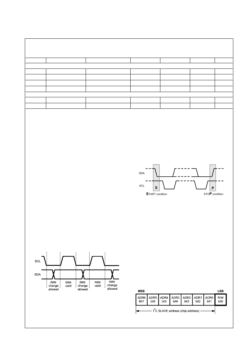
C DATA VALIDITY
The data on SDA line must be stable during the HIGH period
of the clock signal (SCL). In other words, state of the data line
can only be changed when CLK is LOW.
30008549
I
2
C Signals: Data Validity
I
2
C START AND STOP CONDITIONS
START and STOP bits classify the beginning and the end of
the I
2
C session. START condition is defined as SDA signal
transitioning from HIGH to LOW while SCL line is HIGH.
STOP condition is defined as the SDA transitioning from LOW
to HIGH while SCL is HIGH. The I
2
C master always generates
START and STOP bits. The I
2
C bus is considered to be busy
after START condition and free after STOP condition. During
data transmission, I
2
C master can generate repeated START
conditions. First START and repeated START conditions are
equivalent, function-wise.
30008550
TRANSFERRING DATA
Every byte put on the SDA line must be eight bits long, with
the most significant bit (MSB) being transferred first. Each
byte of data has to be followed by an acknowledge bit. The
acknowledge related clock pulse is generated by the master.
The transmitter releases the SDA line (HIGH) during the ac-
knowledge clock pulse. The receiver must pull down the SDA
line during the 9
th
clock pulse, signifying an acknowledge. A
receiver which has been addressed must generate an ac-
knowledge after each byte has been received.
After the START condition, the I
2
C master sends a chip ad-
dress. This address is seven bits long followed by an eighth
bit which is a data direction bit (R/W). The LP39542 address
is 54h or 55H as selected with ADDR_SEL pin.
I
2
C address
for LP39542 is 54H when ADDR_SEL=0 and 55H when
ADDR_SEL=1
. For the eighth bit, a “0” indicates a WRITE
and a “1” indicates a READ. The second byte selects the reg-
ister to which the data will be written. The third byte contains
data to write to the selected register.
30008551
I
2
C Chip Address
www.national.com
32
L
相關(guān)PDF資料 |
PDF描述 |
|---|---|
| LP39542TL | Advanced Lighting Management Unit |
| LP39542TLX | Advanced Lighting Management Unit |
| LP3954 | Advanced Lighting Management Unit |
| LP3954RL | Advanced Lighting Management Unit |
| LP3954RLX | Advanced Lighting Management Unit |
相關(guān)代理商/技術(shù)參數(shù) |
參數(shù)描述 |
|---|---|
| LP39542RLX/NOPB | 功能描述:LED照明驅(qū)動器 RoHS:否 制造商:STMicroelectronics 輸入電壓:11.5 V to 23 V 工作頻率: 最大電源電流:1.7 mA 輸出電流: 最大工作溫度: 安裝風(fēng)格:SMD/SMT 封裝 / 箱體:SO-16N |
| LP39542TL | 制造商:NSC 制造商全稱:National Semiconductor 功能描述:Advanced Lighting Management Unit |
| LP39542TL/NOPB | 功能描述:LED照明驅(qū)動器 RoHS:否 制造商:STMicroelectronics 輸入電壓:11.5 V to 23 V 工作頻率: 最大電源電流:1.7 mA 輸出電流: 最大工作溫度: 安裝風(fēng)格:SMD/SMT 封裝 / 箱體:SO-16N |
| LP39542TLX | 制造商:NSC 制造商全稱:National Semiconductor 功能描述:Advanced Lighting Management Unit |
| LP39542TLX/NOPB | 功能描述:LED照明驅(qū)動器 RoHS:否 制造商:STMicroelectronics 輸入電壓:11.5 V to 23 V 工作頻率: 最大電源電流:1.7 mA 輸出電流: 最大工作溫度: 安裝風(fēng)格:SMD/SMT 封裝 / 箱體:SO-16N |
發(fā)布緊急采購,3分鐘左右您將得到回復(fù)。