- 您現(xiàn)在的位置:買賣IC網(wǎng) > PDF目錄384605 > LMX9830 (National Semiconductor Corporation) BluetoothTM Serial Port Module PDF資料下載
參數(shù)資料
| 型號: | LMX9830 |
| 廠商: | National Semiconductor Corporation |
| 英文描述: | BluetoothTM Serial Port Module |
| 中文描述: | 藍牙串口模塊 |
| 文件頁數(shù): | 15/46頁 |
| 文件大?。?/td> | 664K |
| 代理商: | LMX9830 |
第1頁第2頁第3頁第4頁第5頁第6頁第7頁第8頁第9頁第10頁第11頁第12頁第13頁第14頁當(dāng)前第15頁第16頁第17頁第18頁第19頁第20頁第21頁第22頁第23頁第24頁第25頁第26頁第27頁第28頁第29頁第30頁第31頁第32頁第33頁第34頁第35頁第36頁第37頁第38頁第39頁第40頁第41頁第42頁第43頁第44頁第45頁第46頁
15
www.national.com
L
8.0 Functional Description
(Continued)
.
8.4 AUXILIARY PORTS
8.4.1 RESET#
There are two reset inputs: RESET_RA# for the radio and
RESET_BB# for the baseband. Both are active low.
There is also a reset output, B_RESET_RA# (Buffered
Radio Reset) active low. This output follows input
RESET_RA#.
When
B_RESET_RA# stays low until the clock has started.
RESET_RA#
is
released,
going
high,
Please see Section 8.5 "System Power Up" on page 15 for
details.
8.4.2 General Purpose I/Os
The LMX9830 offers 3 pins which either can be used as
indication and configuration pins or can be used for Gen-
eral Purpose functionality. The selection is made out of set-
tings derived out of the power up sequence.
In General Purpose configuration the pins are controlled
hardware specific commands giving the ability to set the
direction, set them to high or low or enable a weak pull-up.
In alternate function the pins have pre-defined indication
functionality. Please see Table 14 on page 15 for a descrip-
tion on the alternate indication functionality.
8.5 SYSTEM POWER UP
In order to correctly power-up the LMX9830 the following
sequence is recommended to be performed:
Apply VCC_IO and VCC to the LMX9830.
The
RESET_RA#
should
RESET_BB# should be driven high at a recommended
time of 1ms after the LMX9830 voltage rails are high. The
LMX9830 is properly reset.
Please see timing diagram, Figure 9 on page 16.
be
driven
high.
Then
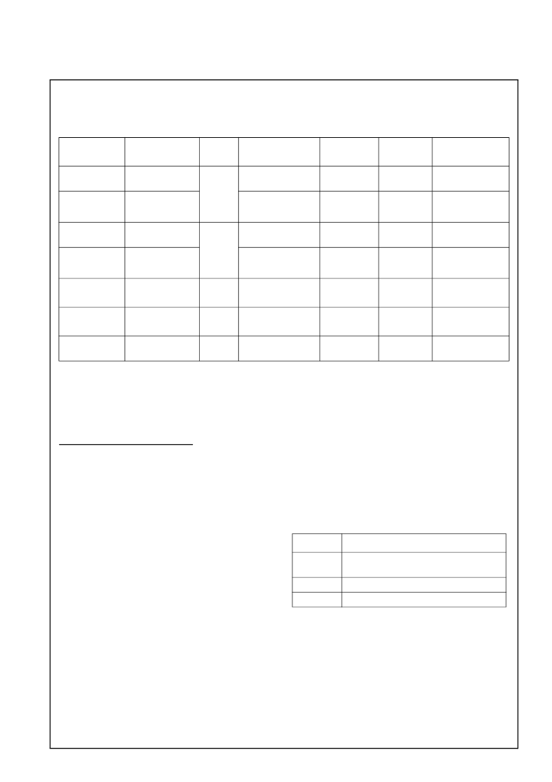
Table 13. Audio path configuration
Audio setting
Interface
Freq
Format
AAI Bit
Clock
AAI Frame
Clock
AAI Frame Sync
Pulse Length
OKI
MSM7717
Advanced audio
interface
ANY
1
8-bit log PCM
(a-law only)
480 KHz
8 KHz
14 Bits
Motorola
MC145483
2
Advanced audio
interface
13-bit linear
480 KHz
8 KHz
13 Bits
OKI
MSM7717
Advanced audio
interface
13MHz
8-bit log PCM
(a-law only)
520 KHz
8 KHz
14 Bits
Motorola
MC145483
3
Advanced audio
interface
13-bit linear
520 KHz
8 KHz
13 Bits
Winbond
W681310
Advanced audio
interface
13MHz
8 bit log PCM
A-law and u-law
520 KHz
8 KHz
14 Bits
Winbond
W681360
Advanced audio
interface
13MHz
13-bit linear
520 KHz
8 KHz
13 Bits
PCM slave
4
Advanced audio
interface
ANY
1
8/16 bits
128 - 1024
KHz
8 KHz
8/16 Bits
1.
2.
For supported frequencies see Table 22 on page 24
Due to internal clock divider limitations the optimum of 512KHz, 8KHz can not be reached. The values are set to the
best possible values. The clock mismatch does not result in any discernible loss in audio quality.
Due to internal clock divider limitations the optimum of 512KHz, 8KHz can not be reached. The values are set to the
best possible values. The clock mismatch does not result in any discernible loss in audio quality.
In PCM slave mode, parameters are stored in NVS. Bit clock and frame clock must be generated by the host interface.
3.
4.
PCM slave configuration example:
PCM slave uses the slot 0, 1 slot per frame, 16 bit linear mode, long frame sync, normal
frame sync. In this case, 0x03E0 should be stored in NVS. See “LMX9830 Software User’s Guide” for more details.
Table 14. Alternate GPIO pin configuration
Pin
Description
OP4/PG4
Operation Mode pin to configure Trans-
port Layer settings during boot-up
PG6
GPIO
PG7
RF Traffic indication
相關(guān)PDF資料 |
PDF描述 |
|---|---|
| LMX9830SM | BluetoothTM Serial Port Module |
| LMX9830SMX | BluetoothTM Serial Port Module |
| LMX9838 | Bluetooth Serial Port Module |
| LMX9838SB | Bluetooth Serial Port Module |
| LMX9838SBX | Bluetooth Serial Port Module |
相關(guān)代理商/技術(shù)參數(shù) |
參數(shù)描述 |
|---|---|
| LMX9830DONGLE | 功能描述:藍牙/802.15.1 開發(fā)工具 LMX9830 BLUETOOTH EVAL KIT RoHS:否 制造商:Panasonic Electronic Components 產(chǎn)品:Bluetooth Evaluation Kit 工具用于評估:PAN1721 頻率:2.4 GHz 接口類型:I2C 工作電源電壓:2 V to 3.6 V |
| LMX9830DONGLE/NOPB | 制造商:Texas Instruments 功能描述:Evaluation Kit For Bluetooth Serial Port Module |
| LMX9830SM | 制造商:NSC 制造商全稱:National Semiconductor 功能描述:BluetoothTM Serial Port Module |
| LMX9830SM/NOPB | 功能描述:射頻收發(fā)器 RoHS:否 制造商:Atmel 頻率范圍:2322 MHz to 2527 MHz 最大數(shù)據(jù)速率:2000 Kbps 調(diào)制格式:OQPSK 輸出功率:4 dBm 類型: 工作電源電壓:1.8 V to 3.6 V 最大工作溫度:+ 85 C 接口類型:SPI 封裝 / 箱體:QFN-32 封裝:Tray |
| LMX9830SMX | 制造商:NSC 制造商全稱:National Semiconductor 功能描述:BluetoothTM Serial Port Module |
發(fā)布緊急采購,3分鐘左右您將得到回復(fù)。