- 您現(xiàn)在的位置:買賣IC網 > PDF目錄44574 > LMX2332UTMX/NOPB (NATIONAL SEMICONDUCTOR CORP) PLL FREQUENCY SYNTHESIZER, 1200 MHz, PDSO20 PDF資料下載
參數資料
| 型號: | LMX2332UTMX/NOPB |
| 廠商: | NATIONAL SEMICONDUCTOR CORP |
| 元件分類: | PLL合成/DDS/VCOs |
| 英文描述: | PLL FREQUENCY SYNTHESIZER, 1200 MHz, PDSO20 |
| 封裝: | 0.173 INCH, PLASTIC, TSSOP-20 |
| 文件頁數: | 27/49頁 |
| 文件大?。?/td> | 4568K |
| 代理商: | LMX2332UTMX/NOPB |
第1頁第2頁第3頁第4頁第5頁第6頁第7頁第8頁第9頁第10頁第11頁第12頁第13頁第14頁第15頁第16頁第17頁第18頁第19頁第20頁第21頁第22頁第23頁第24頁第25頁第26頁當前第27頁第28頁第29頁第30頁第31頁第32頁第33頁第34頁第35頁第36頁第37頁第38頁第39頁第40頁第41頁第42頁第43頁第44頁第45頁第46頁第47頁第48頁第49頁
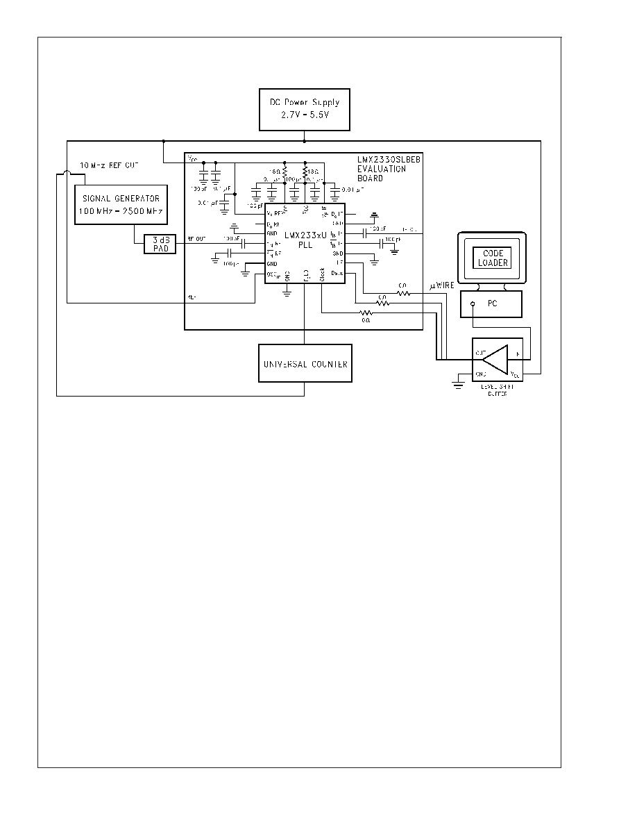
Test Setups (Continued)
LMX233xU f
IN Sensitivity Test Setup
10136640
The block diagram above illustrates the setup required to
measure the LMX233xU device’s RF input sensitivity level.
The
same
setup
is
used
for
the
LMX2330TMEB/
LMX2330SLEEB Evaluation Boards. The IF input sensitivity
test setup is similar to the RF sensitivity test setup. The
purpose of this test is to measure the acceptable signal level
to the f
IN RF input of the PLL chip. Outside the acceptable
signal range, the feedback divider begins to divide incor-
rectly and miscount the frequency.
The setup uses an open loop configuration. A power supply
is connected to V
cc and swept from 2.7V to 5.5V. The IF PLL
is powered down (PWDN IF Bit = 1). By means of a signal
generator, an RF signal is applied to the f
IN RF pin. The 3 dB
pad provides a 50
match between the PLL and the signal
generator. The OSC
in pin is tied to Vcc. The N value is
typically set to 10000 in Code Loader, i.e. RF N_CNTRB
Word = 156 and RF N_CNTRA Word = 16 for PRE RF Bit =
1 (LMX2330U) or PRE RF = 0 (LMX2331U and LMX2332U).
The feedback divider output is routed to the F
oLD pin by
selecting the RF PLL N Divider Output word (F
oLD Word =
6 or 14) in Code Loader. A Universal Counter is connected to
the F
oLD pin and tied to the 10 MHz reference output of the
signal generator. The output of the feedback divider is thus
monitored and should be equal to f
IN RF/N.
The f
IN RF input frequency and power level are then swept
with the signal generator. The measurements are repeated
at different temperatures, namely T
A = -40C, +25C, and
+85C. Sensitivity is reached when the frequency error of the
divided RF input is greater than or equal to 1 Hz. The power
attenuation from the cable and the 3 dB pad must be ac-
counted for. The feedback divider will actually miscount if too
much or too little power is applied to the f
IN RF input.
Therefore, the allowed input power level will be bounded by
the upper and lower sensitivity limits. In a typical application,
if the power level to the f
IN RF input approaches the sensi-
tivity limits, this can introduce spurs and degradation in
phase noise. When the power level gets even closer to these
limits, or exceeds it, then the RF PLL loses lock.
LMX2330U/LMX2331U/LMX2332U
www.national.com
33
相關PDF資料 |
PDF描述 |
|---|---|
| LMX2332UTM/NOPB | PLL FREQUENCY SYNTHESIZER, 1200 MHz, PDSO20 |
| LMX2331UTM/NOPB | PLL FREQUENCY SYNTHESIZER, 2000 MHz, PDSO20 |
| LMX2331USLEX | PLL FREQUENCY SYNTHESIZER, 2000 MHz, PQCC24 |
| LMX2330UTMX/NOPB | PLL FREQUENCY SYNTHESIZER, 2500 MHz, PDSO20 |
| LMX2335LTMX/NOPB | PLL FREQUENCY SYNTHESIZER, 1100 MHz, PDSO16 |
相關代理商/技術參數 |
參數描述 |
|---|---|
| LMX2334ATMX | 制造商:Rochester Electronics LLC 功能描述:- Bulk |
| LMX2335 | 制造商:NSC 制造商全稱:National Semiconductor 功能描述:PLLatinum⑩ Dual Frequency Synthesizer for RF Personal Communications |
| LMX2335 WAF | 制造商:Texas Instruments 功能描述: |
| LMX2335L | 制造商:未知廠家 制造商全稱:未知廠家 功能描述:無線通訊 |
| LMX2335LM | 制造商:Rochester Electronics LLC 功能描述:- Bulk |
發(fā)布緊急采購,3分鐘左右您將得到回復。