- 您現(xiàn)在的位置:買賣IC網(wǎng) > PDF目錄369797 > LM9820 PDF資料下載
參數(shù)資料
| 型號(hào): | LM9820 |
| 文件頁數(shù): | 4/20頁 |
| 文件大小: | 245K |
| 代理商: | LM9820 |
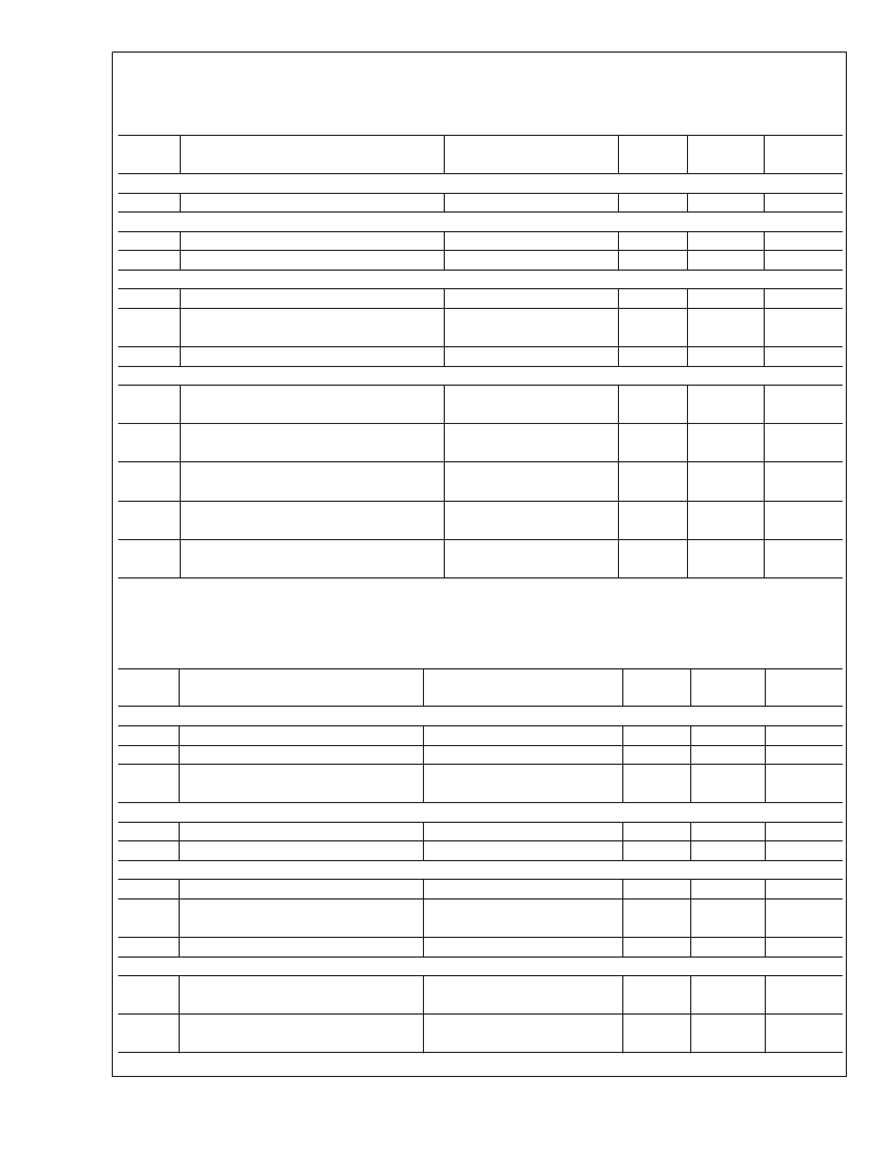
LM9810 Electrical Characteristics
(Continued)
The following specifications apply for AGND = DGND = 0V, V
= V
= +5.0V
, f
= 24 MHz, R
= 25
.
Boldface limits
apply for T
= T
J
= T
MIN
to T
MAX
; all other limits T
A
= T
J
= 25C. All LSB limits are in units of the LM9810’s 10-bit ADC.
(Notes 7, 8, 12)
Symbol
Parameter
Conditions
Typical
(Note 9)
Limits
(Note 10)
Units
(Limits)
ADC CHARACTERISTICS
DNL
Differential Non-Linearity
FULL CHANNEL LINEARITY
(Note 14)
INL
Integral Non-Linearity Error (Note 11)
DNL
Differential Non-Linearity
STATIC OFFSET DAC CHARACTERISTICS
Monotonicity
Offset DAC LSB Size
±
0.25
±
1.0
LSB (max)
±
0.9
±
0.40
LSB
LSB
6
bits (min)
LSB (min)
LSB(max)
LSB (min)
PGA Gain = 1
5
3.4
6.4
±
140
Offset DAC Adjustment Range
SYSTEM CHARACTERISTICS (SEE SECTION 1.7.1, INTERNAL OFFSETS)
C
Analog Channel Gain Constant
(ADC Codes/V)
V
OS1
Pre-Boost Analog Channel Offset Error,
CCD Mode
V
OS1
Pre-Boost Analog Channel Offset Error,
CIS Mode
V
OS2
Pre-PGA Analog Channel Offset Error
PGA Gain = 1
±
150
Includes Voltage Reference
Variation, Gain Setting = 1
502
468
532
-7.2
+15.7
-6.5
+15.2
-28
+5.3
-30.6
+7.3
LSB (min)
LSB (max)
LSB (min)
LSB (max)
LSB (min)
LSB (max)
LSB (min)
LSB (max)
LSB (min)
LSB (max)
4.4
4.5
-10
V
OS3
Post-PGA Analog Channel Offset Error
-11
LM9820 Electrical Characteristics
The following specifications apply for AGND = DGND = 0V, V
= V
= +5.0V
, f
= 24 MHz, R
= 25
.
Boldface limits
apply for T
= T
J
= T
MIN
to T
MAX
; all other limits T
A
= T
J
= 25C. All LSB limits are in units of the LM9810’s 12-bit ADC.
(Notes 7, 8, 12)
Symbol
Parameter
Conditions
Typical
(Note 9)
Limits
(Note 10)
Units
(Limits)
ADC CHARACTERISTICS
Resolution with No Missing Codes
INL
Integral Non-Linearity Error (Note 11)
DNL
Differential Non-Linearity
12
±
4.0
+1.75
-1.0
bits (min)
LSB (max)
LSB (max)
±
1.1
±
0.6
FULL CHANNEL LINEARITY
(Note 14)
INL
Integral Non-Linearity Error (Note 11)
DNL
Differential Non-Linearity
STATIC OFFSET DAC CHARACTERISTICS
Monotonicity
Offset DAC LSB Size
±
3.4
±
0.65
LSB
LSB
6
bits (min)
LSB (min)
LSB(max)
LSB (min)
PGA Gain = 1
20
14
26
Offset DAC Adjustment Range
SYSTEM CHARACTERISTICS (SEE SECTION 1.7.1, INTERNAL OFFSETS)
C
Analog Channel Gain Constant
(ADC Codes/V)
V
OS1
Pre-Boost Analog Channel Offset Error,
CCD Mode
PGA Gain = 1
±
590
±
575
Includes Voltage Reference
Variation, Gain Setting = 1
2008
1873
2129
-32.1
+68.9
LSB (min)
LSB (max)
LSB (min)
LSB (max)
17.6
L
www.national.com
4
相關(guān)PDF資料 |
PDF描述 |
|---|---|
| LM9822CCWM | Signal Conditioner |
| LM9822CCWMX | Signal Conditioner |
| LM9823 | |
| LMA110 | .5-6 GHz MESFET Amplifier |
| LMA110A | .5-6 GHz MESFET Amplifier |
相關(guān)代理商/技術(shù)參數(shù) |
參數(shù)描述 |
|---|---|
| LM9820CCWM | 制造商:NSC 制造商全稱:National Semiconductor 功能描述:LM9810/20 10/12-Bit Image Sensor Processor Analog Front End |
| LM9820CCWMX | 制造商:NSC 制造商全稱:National Semiconductor 功能描述:LM9810/20 10/12-Bit Image Sensor Processor Analog Front End |
| LM9822 | 制造商:NSC 制造商全稱:National Semiconductor 功能描述:LM9822 3 Channel 42-Bit Color Scanner Analog Front End |
| LM9822CCWM | 制造商:Rochester Electronics LLC 功能描述: 制造商:Texas Instruments 功能描述: |
| LM9822CCWM/NOPB | 功能描述:ADC / DAC多通道 RoHS:否 制造商:Texas Instruments 轉(zhuǎn)換速率: 分辨率:8 bit 接口類型:SPI 電壓參考: 電源電壓-最大:3.6 V 電源電壓-最小:2 V 最大工作溫度:+ 85 C 安裝風(fēng)格:SMD/SMT 封裝 / 箱體:VQFN-40 |
發(fā)布緊急采購,3分鐘左右您將得到回復(fù)。