- 您現(xiàn)在的位置:買賣IC網(wǎng) > PDF目錄44572 > LM5008MMXEP (NATIONAL SEMICONDUCTOR CORP) 0.61 A SWITCHING REGULATOR, 600 kHz SWITCHING FREQ-MAX, PDSO8 PDF資料下載
參數(shù)資料
| 型號(hào): | LM5008MMXEP |
| 廠商: | NATIONAL SEMICONDUCTOR CORP |
| 元件分類: | 穩(wěn)壓器 |
| 英文描述: | 0.61 A SWITCHING REGULATOR, 600 kHz SWITCHING FREQ-MAX, PDSO8 |
| 封裝: | PLASTIC, MSOP-8 |
| 文件頁(yè)數(shù): | 2/15頁(yè) |
| 文件大小: | 662K |
| 代理商: | LM5008MMXEP |
第1頁(yè)當(dāng)前第2頁(yè)第3頁(yè)第4頁(yè)第5頁(yè)第6頁(yè)第7頁(yè)第8頁(yè)第9頁(yè)第10頁(yè)第11頁(yè)第12頁(yè)第13頁(yè)第14頁(yè)第15頁(yè)
Current Limit
The LM5008EP contains an intelligent current limit OFF
timer. If the current in the Buck switch exceeds 0.5A the
present cycle is immediately terminated, and a non-
resetable OFF timer is initiated. The length of off-time is
controlled by an external resistor (R
CL) and the FB voltage
(see Figure 5). When FB = 0V, a maximum off-time is re-
quired, and the time is preset to 35s. This condition occurs
when the output is shorted, and during the initial part of
start-up. This amount of time ensures safe short circuit op-
eration up to the maximum input voltage of 95V. In cases of
overload where the FB voltage is above zero volts (not a
short circuit) the current limit off-time will be less than 35s.
Reducing the off-time during less severe overloads reduces
the amount of foldback, recovery time, and the start-up time.
The off-time is calculated from the following equation:
T
OFF =10
-5 / (0.285 + (V
FB /6.35x10
-6 xR
CL))
(3)
The current limit sensing circuit is blanked for the first 50-
70ns of each on-time so it is not falsely tripped by the current
surge which occurs at turn-on. The current surge is required
by the re-circulating diode (D1) for its turn-off recovery.
N - Channel Buck Switch and
Driver
The LM5008EP integrates an N-Channel Buck switch and
associated floating high voltage gate driver. The gate driver
circuit works in conjunction with an external bootstrap ca-
pacitor and an internal high voltage diode. A 0.01F ceramic
capacitor (C4) connected between the BST pin and SW pin
provides the voltage to the driver during the on-time.
During each off-time, the SW pin is at approximately 0V, and
the bootstrap capacitor charges from Vcc through the inter-
nal diode. The minimum OFF timer, set to 300ns, ensures a
minimum time each cycle to recharge the bootstrap capaci-
tor.
An external re-circulating diode (D1) carries the inductor
current after the internal Buck switch turns off. This diode
must be of the Ultra-fast or Schottky type to minimize turn-on
losses and current over-shoot.
Thermal Protection
The LM5008EP should be operated so the junction tempera-
ture does not exceed 125C during normal operation. An
internal Thermal Shutdown circuit is provided to protect the
LM5008EP in the event of a higher than normal junction
temperature. When activated, typically at 165C, the control-
ler is forced into a low power reset state, disabling the buck
switch and the V
CC regulator. This feature prevents cata-
strophic failures from accidental device overheating. When
the junction temperature reduces below 140C (typical hys-
teresis = 25C), the Vcc regulator is enabled, and normal
operation is resumed.
Applications Information
SELECTION OF EXTERNAL COMPONENTS
A guide for determining the component values will be illus-
trated with a design example. Refer to Figure 1. The follow-
ing steps will configure the LM5008EP for:
Input voltage range (Vin): 12V to 95V
Output voltage (V
OUT1): 10V
Load current (for continuous conduction mode): 100 mA
to 300 mA
Maximum ripple at V
OUT2: 100 mVp-p at maximum input
voltage
R1 and R2: From Figure 1,V
OUT1 =VFB x (R1 + R2) / R2,
and since V
FB = 2.5V, the ratio of R1 to R2 calculates as 3:1.
Standard values of 3.01 k
(R1) and 1.00 k (R2) are
chosen. Other values could be used as long as the 3:1 ratio
is maintained. The selected values, however, provide a small
amount of output loading (2.5 mA) in the event the main load
is disconnected. This allows the circuit to maintain regulation
until the main load is reconnected.
F
s and RON: The recommended operating frequency range
for the LM5008EP is 50kHz to 600 kHz. Unless the applica-
tion requires a specific frequency, the choice of frequency is
generally a compromise since it affects the size of L1 and
C2, and the switching losses. The maximum allowed fre-
quency, based on a minimum on-time of 400 ns, is calcu-
lated from:
F
MAX =VOUT /(VINMAX x 400ns)
For this exercise, Fmax = 263kHz. From equation 1, R
ON
calculates to 304 k
. A standard value 357 k resistor will
be used to allow for tolerances in equation 1, resulting in a
frequency of 224kHz.
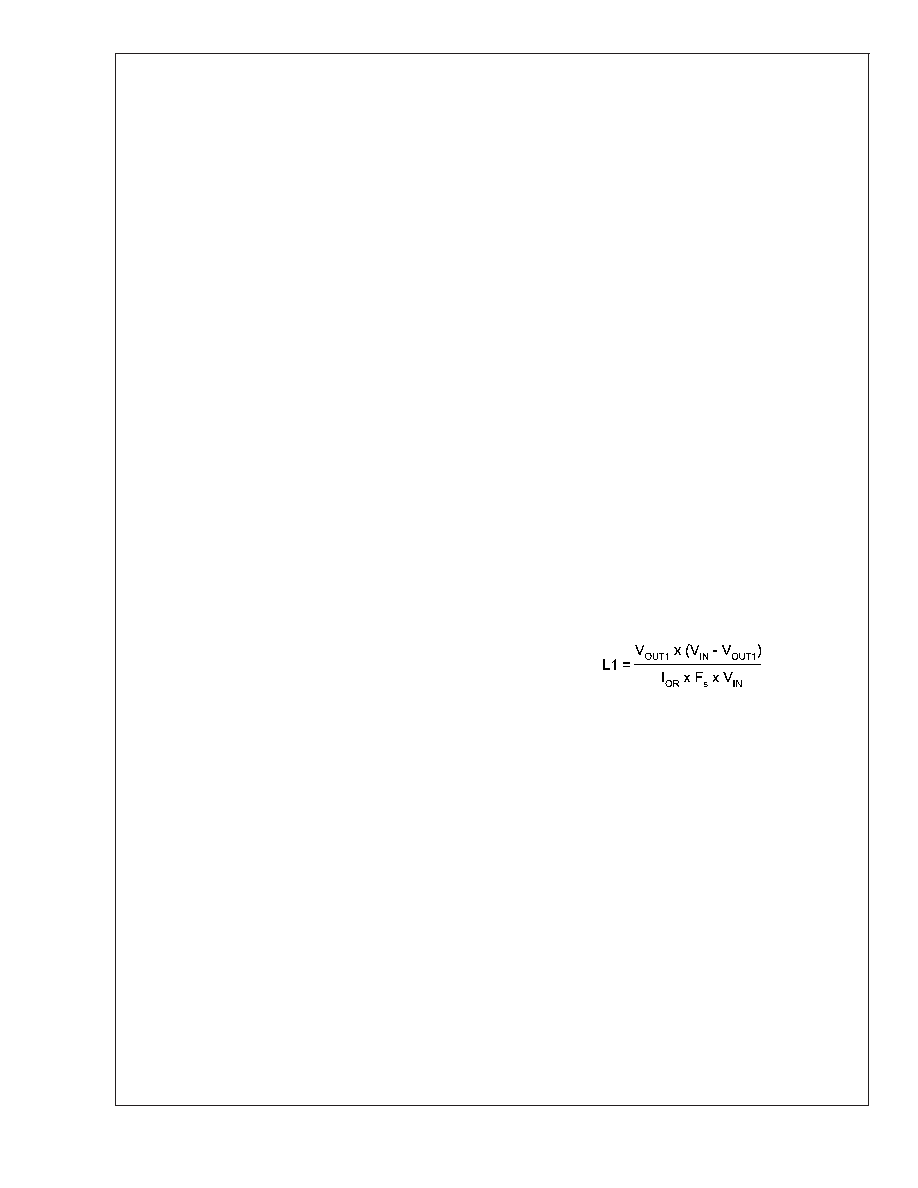
L1: The main parameter affected by the inductor is the
output current ripple amplitude. The choice of inductor value
therefore depends on both the minimum and maximum load
currents, keeping in mind that the maximum ripple current
occurs at maximum Vin.
a) Minimum load current: To maintain continuous conduc-
tion at minimum Io (100 mA), the ripple amplitude (I
OR) must
be less than 200 mA p-p so the lower peak of the waveform
does not reach zero. L1 is calculated using the following
equation:
At Vin = 95V, L1(min) calculates to 200 H. The next larger
standard value (220 H) is chosen and with this value I
OR
calculates to 181 mA p-p at Vin = 95V, and 34 mA p-p at Vin
= 12V.
b) Maximum load current: At a load current of 300 mA, the
peak of the ripple waveform must not reach the minimum
guaranteed value of the LM5008EP’s current limit threshold
(410 mA). Therefore the ripple amplitude must be less than
220 mA p-p, which is already satisfied in the above calcula-
tion. With L1 = 220 H, at maximum Vin and Io, the peak of
the ripple will be 391 mA. While L1 must carry this peak
current without saturating or exceeding its temperature rat-
ing, it also must be capable of carrying the maximum guar-
anteed value of the LM5008EP’s current limit threshold (610
mA) without saturating, since the current limit is reached
during startup.
The DC resistance of the inductor should be as low as
possible. For example, if the inductor’s DCR is one ohm, the
power dissipated at maximum load current is 0.09W. While
small, it is not insignificant compared to the load power of
3W.
C3: The capacitor on the V
CC output provides not only noise
filtering and stability, but its primary purpose is to prevent
LM5008EP
www.national.com
10
相關(guān)PDF資料 |
PDF描述 |
|---|---|
| LM5008SD/NOPB | 0.61 A SWITCHING REGULATOR, DSO8 |
| LM5008SDEP | 0.61 A SWITCHING REGULATOR, 600 kHz SWITCHING FREQ-MAX, PDSO8 |
| LM5008SDX | 0.61 A SWITCHING REGULATOR, DSO8 |
| LM5027AMH | SWITCHING CONTROLLER, 1000 kHz SWITCHING FREQ-MAX, PDSO20 |
| LM5027AMHX | SWITCHING CONTROLLER, 1000 kHz SWITCHING FREQ-MAX, PDSO20 |
相關(guān)代理商/技術(shù)參數(shù) |
參數(shù)描述 |
|---|---|
| LM5008SD | 功能描述:直流/直流開(kāi)關(guān)轉(zhuǎn)換器 RoHS:否 制造商:STMicroelectronics 最大輸入電壓:4.5 V 開(kāi)關(guān)頻率:1.5 MHz 輸出電壓:4.6 V 輸出電流:250 mA 輸出端數(shù)量:2 最大工作溫度:+ 85 C 安裝風(fēng)格:SMD/SMT |
| LM5008SD/NOPB | 功能描述:直流/直流開(kāi)關(guān)轉(zhuǎn)換器 RoHS:否 制造商:STMicroelectronics 最大輸入電壓:4.5 V 開(kāi)關(guān)頻率:1.5 MHz 輸出電壓:4.6 V 輸出電流:250 mA 輸出端數(shù)量:2 最大工作溫度:+ 85 C 安裝風(fēng)格:SMD/SMT |
| LM5008SDC | 功能描述:直流/直流開(kāi)關(guān)轉(zhuǎn)換器 RoHS:否 制造商:STMicroelectronics 最大輸入電壓:4.5 V 開(kāi)關(guān)頻率:1.5 MHz 輸出電壓:4.6 V 輸出電流:250 mA 輸出端數(shù)量:2 最大工作溫度:+ 85 C 安裝風(fēng)格:SMD/SMT |
| LM5008SDC/NOPB | 功能描述:直流/直流開(kāi)關(guān)轉(zhuǎn)換器 RoHS:否 制造商:STMicroelectronics 最大輸入電壓:4.5 V 開(kāi)關(guān)頻率:1.5 MHz 輸出電壓:4.6 V 輸出電流:250 mA 輸出端數(shù)量:2 最大工作溫度:+ 85 C 安裝風(fēng)格:SMD/SMT |
| LM5008SDCX | 功能描述:直流/直流開(kāi)關(guān)轉(zhuǎn)換器 RoHS:否 制造商:STMicroelectronics 最大輸入電壓:4.5 V 開(kāi)關(guān)頻率:1.5 MHz 輸出電壓:4.6 V 輸出電流:250 mA 輸出端數(shù)量:2 最大工作溫度:+ 85 C 安裝風(fēng)格:SMD/SMT |
發(fā)布緊急采購(gòu),3分鐘左右您將得到回復(fù)。