- 您現(xiàn)在的位置:買賣IC網(wǎng) > PDF目錄358865 > LM4549 (National Semiconductor Corporation) AC ’97 Rev 2.1 Codec with Sample Rate Conversion and National 3D Sound PDF資料下載
參數(shù)資料
| 型號: | LM4549 |
| 廠商: | National Semiconductor Corporation |
| 元件分類: | Codec |
| 英文描述: | AC ’97 Rev 2.1 Codec with Sample Rate Conversion and National 3D Sound |
| 中文描述: | 交流\u0026#39;97活2.1編解碼器的采樣率轉(zhuǎn)換和國家3D聲音 |
| 文件頁數(shù): | 13/18頁 |
| 文件大?。?/td> | 324K |
| 代理商: | LM4549 |
Application Information
(Continued)
Bit
Description
Right
Playback
PCM Data
Comment
11
1 = Right PCM Data is
valid.
SDATA_OUT Slot 1: Control Address
Slot 1 is used both to write to the LM4549 registers as well
as read back a register’s current value. The MSB of Slot 1
(bit 19) signifies whether the current control operation is a
read or a write. Bits 18 through 12 are used to specify the
register address of the read or write operation. The least sig-
nificant twelve bits are reserved and should be stuffed with
zeros by the AC’97 controller.
Bits
19
Description
Read/Write
Control
Register
Reserved
Comment
0 = Read, 1 = Write
Identifies the Control
Register
Set to
″
0
″
18:12
11:0
SDATA_OUT Slot 2: Control Data
Slot 2 is used to transmit 16 bit control data to the LM4549 in
the event that the current operation is a write operation. The
least significant four bits should be stuffed with zeros by the
AC ’97 controller. If the current operation is a register read,
the entire slot, bits 19 through 0 should be stuffed with zeros.
Bits
Description
Control
Register Write
Data
Reserved
Comment
19:4
Set bits to
″
0
″
if read
operation
3:0
Set to
″
0
″
SDATA_OUT Slot 3: PCM Playback Left Channel
Slot 3 is a 20 bit field used to transmit data intended for the
left DAC on the LM4549. Any unused bits should be padded
with zeros. The LM4549 DAC’s have 18 bit resolution and
thus will use the first 18 bits of the 20 bit PCM stream.
Bits
Description
PCM Audio
Data for Left
DAC
Comment
19:0
Set unused bits to
″
0
″
SDATA_OUT Slot 4: PCM Playback Right Channel
Slot 4 is a 20 bit field used to transmit data intended for the
right DAC on the LM4549. Any unused bits should be pad-
ded with zeros. The LM4549 DAC’s have 18 bit resolution
and thus will use the first 18 bits of the 20 bit PCM stream.
Bits
Description
PCM Audio
Data for Right
DAC
Comment
19:0
Set unused bits to
″
0
″
SDATA_OUT Slots 5-12: Reserved
Set these SDATA_OUT slots to
″
0
″
as they are not currently
implemented and are reserved for future use.
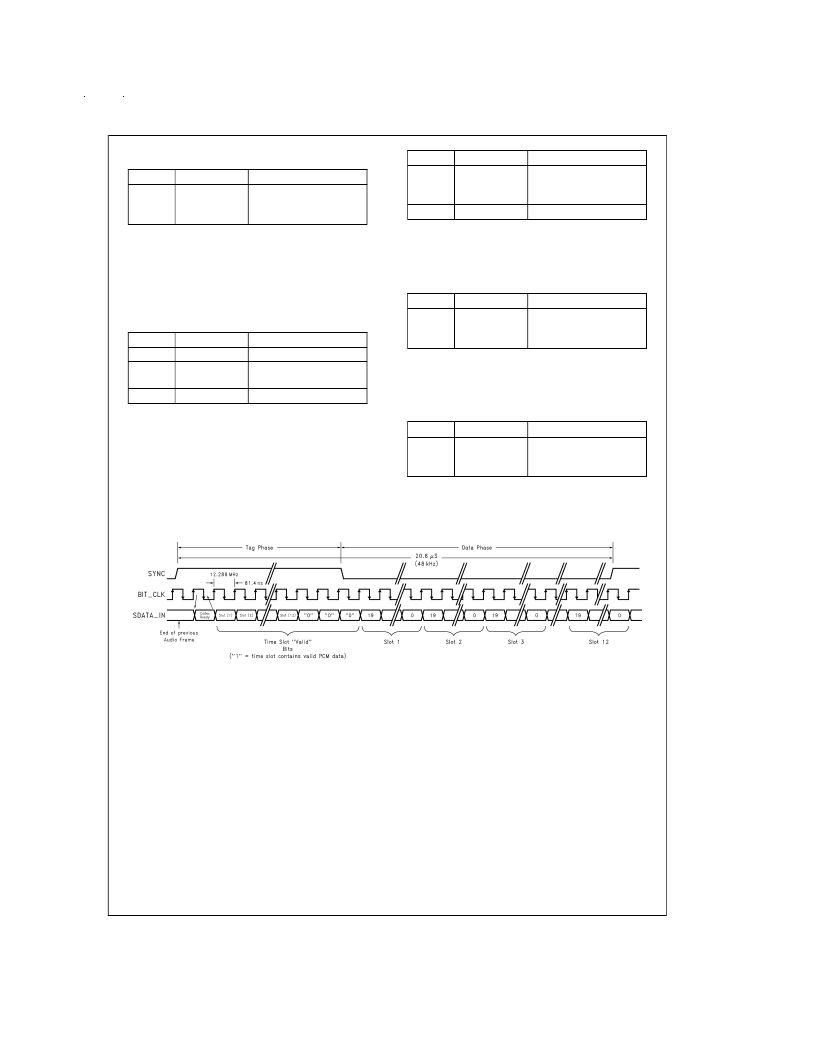
AC Link Input Frame: SDATA_IN (input to controller,
output from LM4549)
The audio input frame (input to the AC ’97 Digital Controller)
contains status and PCM data from the LM4549 control reg-
isters and stereo ADC. The Tag slot, slot 0, contains 16 bits
that tell the AC ’97 Digital Controller whether the LM4549 is
ready and the validity of data from certain device subsec-
tions.
A new audio input frame is signaled with a low to high tran-
sition of SYNC. SYNC is synchronous to the rising edge of
BIT_CLK. On the next rising edge of BIT_CLK, the LM4549
drives SDATA_IN with the first bit of slot 0. The Digital Con-
troller samples SDATA_IN on the falling edge of BIT_CLK.
The LM4549 will continue outputting the SDATA_IN stream
on each successive rising edge of BIT_CLK. The LM4549
outputs data MSB first, in a MSB justified format.All reserved
bits and slots are stuffed with
″
0
″
’s by the LM4549.
SDATA_IN Slot 0: Codec Status Bits
The first bit of SDATA_IN Slot 0 (bit 15) indicates when the
Codec is ready. The digital controller must probe further to
see which other subsections are ready.
DS101035-8
FIGURE 6. AC Link Audio Input Frame
www.national.com
13
相關(guān)PDF資料 |
PDF描述 |
|---|---|
| LM4558 | DUAL OPERATIONAL AMPLIFIERS |
| LM4560VJD | Advanced PCI Audio Accelerator |
| LM4560 | Advanced PCI Audio Accelerator |
| LM45BIM3 | SOT-23 Precision Centigrade Temperature Sensors |
| LM45BIM3X | SOT-23 Precision Centigrade Temperature Sensors |
相關(guān)代理商/技術(shù)參數(shù) |
參數(shù)描述 |
|---|---|
| LM4549A | 制造商:NSC 制造商全稱:National Semiconductor 功能描述:AC ’97 Rev 2.1 Codec with Sample Rate Conversion and National 3D Sound |
| LM4549AVH | 制造商:Rochester Electronics LLC 功能描述:AC97 REV2.1 CODEC - Bulk 制造商:OC White Company 功能描述:Audio Codec 2ADC / 2DAC 18-Bit 48-Pin LQFP Tray |
| LM4549AVH WAF | 制造商:Texas Instruments 功能描述: |
| LM4549AVH/NOPB | 制造商:Texas Instruments 功能描述:Audio Codec 2ADC / 2DAC 18-Bit 48-Pin LQFP Tray |
| LM4549AVHX | 制造商:Rochester Electronics LLC 功能描述:AC97 REV2.1 CODEC - Bulk |
發(fā)布緊急采購,3分鐘左右您將得到回復(fù)。