- 您現(xiàn)在的位置:買賣IC網(wǎng) > PDF目錄44551 > LM2702MT-ADJ/NOPB (NATIONAL SEMICONDUCTOR CORP) 2.6 A SWITCHING REGULATOR, 720 kHz SWITCHING FREQ-MAX, PDSO16 PDF資料下載
參數(shù)資料
| 型號: | LM2702MT-ADJ/NOPB |
| 廠商: | NATIONAL SEMICONDUCTOR CORP |
| 元件分類: | 穩(wěn)壓器 |
| 英文描述: | 2.6 A SWITCHING REGULATOR, 720 kHz SWITCHING FREQ-MAX, PDSO16 |
| 封裝: | TSSOP-16 |
| 文件頁數(shù): | 11/21頁 |
| 文件大小: | 1197K |
| 代理商: | LM2702MT-ADJ/NOPB |
Operation (Continued)
Vcom AND Gamma COMPENSATION
The architecture used for the amplifiers in the LM2702 re-
quires external compensation on the output. Depending on
the equivalent capacitive load of the TFT-LCD panel, exter-
nal components at the amplifier outputs may or may not be
necessary. If the capacitance presented by the load is equal
to or greater than 5nF no external components are needed
as the TFT-LCD panel will act as compensation itself. Dis-
tributed resistive and capacitive loads enhance stability and
increase performance of the amplifiers. If the capacitance
presented by the load is less than 5nF external components
will be required as the load itself will not ensure stability. No
external compensation in this case will lead to oscillation of
the amplifier and an increase in power consumption. A single
5nF or greater capacitor on the output will ensure a stable
amplifier with no oscillations. For applications requiring a
higher slew rate, a good choice for compensation is to add a
50
(R
COM or RGAMMA) in series with a 1nF (CCOM or
C
GAMMA) capacitor from the output of the amplifier to ground.
This allows for driving zero to infinite capacitance loads with
no oscillations, minimal overshoot, and a higher slew rate
than using a large capacitor. The high phase margin created
by the external compensation will guarantee stability and
good performance for all conditions.
For noise sensitive applications greater output capacitance
may be desired. When the power supply for the amplifiers
(AV
IN) is connected to the output of the switching regulator,
the output ripple of the regulator will produce ripple at the
output of the amplifiers.
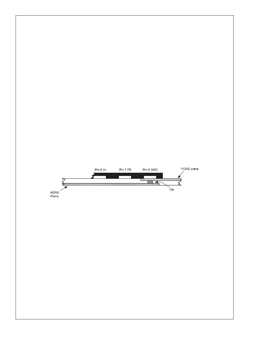
LAYOUT CONSIDERATIONS
The LM2702 uses a single ground connection, GND. The
feedback, softstart, delay, and compensation networks
should be connected directly to a dedicated analog ground
plane and this ground plane must connect to the GND pin, as
shown in Figure 3. If no analog ground plane is available
then the ground connections of the feedback, softstart, de-
lay, and compensation networks must tie directly to the GND
pin, as show in Figure 4. Connecting these networks to the
PGND plane can inject noise into the system and effect
performance.
The input bypass capacitor C
IN must be placed close to the
IC. This will reduce copper trace resistance which effects
input voltage ripple of the IC. For additional input voltage
filtering, a 100nF bypass capacitor can be placed in parallel
with C
IN, close to the VIN pin, to shunt any high frequency
noise to ground. The output capacitor, C
OUT, should also be
placed close to the IC. Any copper trace connections for the
C
OUT capacitor can increase the series resistance, which
directly effects output voltage ripple and efficiency. The feed-
back network, resistors R1 and R2, should be kept close to
the FB pin, and away from the inductor, to minimize copper
trace connections that can inject noise into the system.
Trace connections made to the inductor and schottky diode
should be minimized to reduce power dissipation and in-
crease overall efficiency.
20051152
FIGURE 3. Multi-Layer Layout
LM2702
www.national.com
19
相關(guān)PDF資料 |
PDF描述 |
|---|---|
| LM27402SQX | SWITCHING CONTROLLER, 1350 kHz SWITCHING FREQ-MAX, QCC16 |
| LM27402MHX | SWITCHING CONTROLLER, 1350 kHz SWITCHING FREQ-MAX, PDSO16 |
| LM2770SD-12157/NOPB | SWITCHED CAPACITOR REGULATOR, 925 kHz SWITCHING FREQ-MAX, DSO10 |
| LM2770SDX-1215/NOPB | SWITCHED CAPACITOR REGULATOR, 925 kHz SWITCHING FREQ-MAX, DSO10 |
| LM2788MM-2.0/NOPB | SWITCHED CAPACITOR REGULATOR, 500 kHz SWITCHING FREQ-MAX, PDSO8 |
相關(guān)代理商/技術(shù)參數(shù) |
參數(shù)描述 |
|---|---|
| LM2702MTX-ADJ | 制造商:NSC 制造商全稱:National Semiconductor 功能描述:TFT Panel Module |
| LM2703 | 制造商:NSC 制造商全稱:National Semiconductor 功能描述:Micropower Step-up DC/DC Converter with 350mA Peak Current Limit |
| LM2703EV | 功能描述:電源管理IC開發(fā)工具 LM2703 EVAL UNIT RoHS:否 制造商:Maxim Integrated 產(chǎn)品:Evaluation Kits 類型:Battery Management 工具用于評估:MAX17710GB 輸入電壓: 輸出電壓:1.8 V |
| LM2703EV/NOPB | 制造商:Texas Instruments 功能描述:Evaluation Board For LM2703 |
| LM2703MFADJ | 制造商:Texas Instruments 功能描述: |
發(fā)布緊急采購,3分鐘左右您將得到回復(fù)。