- 您現(xiàn)在的位置:買賣IC網(wǎng) > PDF目錄385474 > LM1209 (National Semiconductor Corporation) 130 MHz/100 MHz RGB Video Amplifier System with Blanking PDF資料下載
參數(shù)資料
| 型號(hào): | LM1209 |
| 廠商: | National Semiconductor Corporation |
| 元件分類: | 運(yùn)動(dòng)控制電子 |
| 英文描述: | 130 MHz/100 MHz RGB Video Amplifier System with Blanking |
| 中文描述: | 130 MHz/100 MHz的RGB視頻信號(hào)放大器系統(tǒng)的沖裁 |
| 文件頁(yè)數(shù): | 19/25頁(yè) |
| 文件大?。?/td> | 434K |
| 代理商: | LM1209 |
第1頁(yè)第2頁(yè)第3頁(yè)第4頁(yè)第5頁(yè)第6頁(yè)第7頁(yè)第8頁(yè)第9頁(yè)第10頁(yè)第11頁(yè)第12頁(yè)第13頁(yè)第14頁(yè)第15頁(yè)第16頁(yè)第17頁(yè)第18頁(yè)當(dāng)前第19頁(yè)第20頁(yè)第21頁(yè)第22頁(yè)第23頁(yè)第24頁(yè)第25頁(yè)
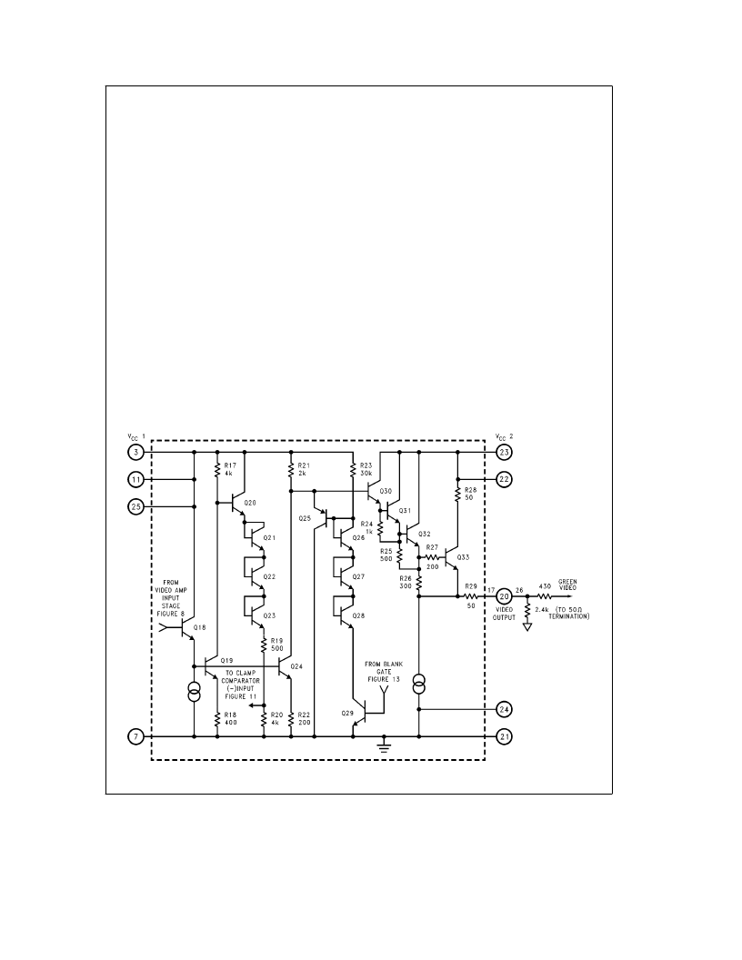
Circuit Description
(Continued)
age of Q29. There are also four diode drops from the base
of Q30 to the output, pin 20. Therefore during blanking pin
20 will be less than 100 mV above ground, enabling the
designer to blank at the cathode of the CRT. R23 is added
to quickly turn off Q25 by discharging its base when the
blanking signal is removed.
Figure 14 also shows the power and ground pins to the
LM1208/LM1209. All the V
CC1
pins (pins 3, 11, 25) are all
internally connected together. A 0.1
m
F bypass capacitor
must be located close to each pin and connected to ground.
Further bypassing is done by a 100
m
F capacitor. This ca-
pacitor needs to be located on the board close to the
LM1208/LM1209. Pins 22 and 23 are the V
CC2
pins. These
pins may need a ferrite bead in series with the input power.
A 10
m
F and a 0.1
m
F bypass capacitors must be located
close to pins 22 and 23. Correct bypassing of pins 22 and
23 is
very important
. If the bypassing is not adequate then
the outputs of the LM1208/LM1209 will have ringing, or
even worse they may oscillate. The ground side of the by-
pass capacitors at pins 22 and 23 must be returned to a
ground plane with no interruptions from other traces be-
tween these capacitors and the ground pins 21 and 24 of
the LM1208/LM1209.
Applications of the LM1208/
LM1209
Figure 15 is the schematic of the demonstration board de-
signed at National.Figure 16 is the actual layout of the dem-
onstration board. Note that the schematic shown in
Figure 15 is almost identical to the schematic shown inFig-
ure 4. The only difference between the two schematics is
that in Figure 15 each channel has individual adjustments
for both drive and cutoff, making this circuit a good design
for monitor applications. Each CRT will have a slightly differ-
ent cutoff voltage for each color, making it necessary to
provide separate adjustments in order to accurately set the
cutoffforeachcolor.ThegainofeachcoloroftheCRTisalso
slightly different; if the color temperature of the display is to
be accurately set then each channel of the LM1208/
LM1209 must have individual gain adjustments. Thus each
channel has its own drive control. Once the drive control is
set, the gain between the three color channels will closely
track as the contrast is adjusted. All the jumpers needed to
design a single sided PC board are shown in the schematic.
The resistors and jumpers with no reference designation are
the connections between the PC board and the connectors
mounted on the PC board. CN1 thru CN8 are BNC connec-
tors.
A 30
X
resistor is in series with each of the video inputs. A
voltage surge may occur at these inputs when either the
inputs are first connected to another system, or when the
system is powered up before the monitor is turned on. If this
voltage surge exceeds the supply voltage (at ground poten-
tial if the monitor is not powered up) of the LM1208/
LM1209, or goes below ground, current will flow through the
parasitic devices of the LM1208/LM1209. This current is
limited by the 30
X
resistors, preventing a potential cata-
strophic failure. A 100
X
resistor is added to the Blank Gate
and Clamp Gate inputs. These two resistors also limit
TL/H/11884–19
FIGURE 14. Simplified Schematic of LM1208/LM1209 Video Amplifier Output Stage with Blank Circuit
http://www.national.com
19
相關(guān)PDF資料 |
PDF描述 |
|---|---|
| LM1212N | 230 MHz Video Amplifier System with OSD Blanking |
| LM1229 | I2C Compatible CMOS TV RGB and Deflection Processor |
| LM1229VEC | I2C Compatible CMOS TV RGB and Deflection Processor |
| LM1229YA | I2C Compatible CMOS TV RGB and Deflection Processor |
| LM1247 | 150 MHz I2C Compatible RGB Preamplifier with Internal 512 Character OSD ROM, 512 Character RAM and 4 DACs |
相關(guān)代理商/技術(shù)參數(shù) |
參數(shù)描述 |
|---|---|
| LM120A-05 | 制造商:SEME-LAB 制造商全稱:Seme LAB 功能描述:1.5 AMP NEGATIVE VOLTAGE REGULATOR |
| LM120AG-05 | 制造商:未知廠家 制造商全稱:未知廠家 功能描述:Analog IC |
| LM120AG-05-8QR-B | 制造商:未知廠家 制造商全稱:未知廠家 功能描述:Voltage Regulator |
| LM120AG-12 | 制造商:未知廠家 制造商全稱:未知廠家 功能描述:Voltage Regulator |
| LM120AG-12-8QR-B | 制造商:未知廠家 制造商全稱:未知廠家 功能描述:Voltage Regulator |
發(fā)布緊急采購(gòu),3分鐘左右您將得到回復(fù)。