- 您現(xiàn)在的位置:買賣IC網(wǎng) > PDF目錄385472 > LH75411N0Q100C0 (NXP Semiconductors N.V.) System-on-Chip PDF資料下載
參數(shù)資料
| 型號: | LH75411N0Q100C0 |
| 廠商: | NXP Semiconductors N.V. |
| 元件分類: | 數(shù)學(xué)處理器 |
| 英文描述: | System-on-Chip |
| 封裝: | LH75401N0Q100C0<SOT486-1 (LQFP144)|<<http://www.nxp.com/packages/SOT486-1.html<1<Always Pb-free,;LH75411N0Q100C0<SOT486-1 (LQFP144)|<<http://www.nxp.com/packages/SOT486-1 |
| 文件頁數(shù): | 41/63頁 |
| 文件大小: | 665K |
| 代理商: | LH75411N0Q100C0 |
第1頁第2頁第3頁第4頁第5頁第6頁第7頁第8頁第9頁第10頁第11頁第12頁第13頁第14頁第15頁第16頁第17頁第18頁第19頁第20頁第21頁第22頁第23頁第24頁第25頁第26頁第27頁第28頁第29頁第30頁第31頁第32頁第33頁第34頁第35頁第36頁第37頁第38頁第39頁第40頁當(dāng)前第41頁第42頁第43頁第44頁第45頁第46頁第47頁第48頁第49頁第50頁第51頁第52頁第53頁第54頁第55頁第56頁第57頁第58頁第59頁第60頁第61頁第62頁第63頁
System-on-Chip
LH75401/LH75411
Preliminary data sheet
Rev. 01
—
16 July 2007
41
NXP Semiconductors
MEMORY CONTROLLER WAVEFORMS
Static Memory Controller Waveforms
Figure 8 shows the waveform and timing for an
External Static Memory Write, with one Wait State. Fig-
ure 9 shows the waveform and timing for an External
Static Memory Write, with two Wait States. Figure 10
shows the waveform and timing for an External Static
Memory Read, with one Wait State.
The SMC supports an nWAIT input that can be used
by an external device to extend the wait time during a
memory access. The SMC samples nWAIT at the
beginning of at the beginning of each system clock
cycle. The system clock cycle in which the nCSx signal
is asserted counts as the first wait state. See Figure 11.
The SMC recognizes that nWAIT is active within 2
clock cycles after it has been asserted. To assure that
the current access (read or write) will be extended by
nWAIT, program at least two wait states for this bank of
memory. If N wait states are programmed, the SMC
holds this state for N system clocks or until the SMC
detects that nWAIT is inactive, whichever occurs last.
As the number of wait states programmed increases,
the amount of delay before nWAIT must be asserted
also increases. If only 2 wait states are programmed,
nWAIT must be asserted in the clock cycle immediately
following the clock cycle during which the nCSx signal
is asserted. Once the SMC detects that the external
device has deactivated nWAIT, the SMC completes its
access in 3 system clock cycles.
The formula for the allowable delay between assert-
ing nCSx and asserting nWAIT is:
tASSERT = (system clock period) × (Wait States - 1)
(where Wait States is from 2 to 31.)
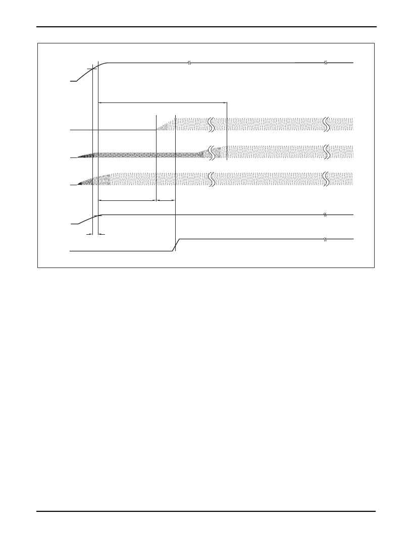
The signal tIDD is shown without a setup time, as
measurements are made from the Address Valid point
and HCLK is an internal signal, shown for reference only.
Figure 7. Power-up Stabilization
LH754xx-100
VDD
XTAL14
XTAL32
PLL
nPOR
tPORH
tOSC14
VDDCmin
tOSC32
tLREG
VDDmin
LREG
相關(guān)PDF資料 |
PDF描述 |
|---|---|
| LH79520N0Q000B1 | System-on-Chip |
| LH79524N0F100A1 | System-on-Chip |
| LH79525N0Q100A1 | System-on-Chip |
| LH7A400N0F000B5 | 32-Bit System-on-Chip |
| LH7A400N0F076B5 | 32-Bit System-on-Chip |
相關(guān)代理商/技術(shù)參數(shù) |
參數(shù)描述 |
|---|---|
| LH75411N0Q100C0,55 | 功能描述:ARM微控制器 - MCU LCD,EXT BUS,ADC,QFP144 RoHS:否 制造商:STMicroelectronics 核心:ARM Cortex M4F 處理器系列:STM32F373xx 數(shù)據(jù)總線寬度:32 bit 最大時(shí)鐘頻率:72 MHz 程序存儲器大小:256 KB 數(shù)據(jù) RAM 大小:32 KB 片上 ADC:Yes 工作電源電壓:1.65 V to 3.6 V, 2 V to 3.6 V, 2.2 V to 3.6 V 工作溫度范圍:- 40 C to + 85 C 封裝 / 箱體:LQFP-48 安裝風(fēng)格:SMD/SMT |
| LH75411N0Q100C0,551 | 制造商:NXP Semiconductors 功能描述: |
| LH75411N0Q100C0;55 | 功能描述:ARM微控制器 - MCU LCD EXT BUS ADC RoHS:否 制造商:STMicroelectronics 核心:ARM Cortex M4F 處理器系列:STM32F373xx 數(shù)據(jù)總線寬度:32 bit 最大時(shí)鐘頻率:72 MHz 程序存儲器大小:256 KB 數(shù)據(jù) RAM 大小:32 KB 片上 ADC:Yes 工作電源電壓:1.65 V to 3.6 V, 2 V to 3.6 V, 2.2 V to 3.6 V 工作溫度范圍:- 40 C to + 85 C 封裝 / 箱體:LQFP-48 安裝風(fēng)格:SMD/SMT |
| LH75411N0Q100C0-S | 功能描述:ARM微控制器 - MCU ARM7 LCD ADC JTAG RoHS:否 制造商:STMicroelectronics 核心:ARM Cortex M4F 處理器系列:STM32F373xx 數(shù)據(jù)總線寬度:32 bit 最大時(shí)鐘頻率:72 MHz 程序存儲器大小:256 KB 數(shù)據(jù) RAM 大小:32 KB 片上 ADC:Yes 工作電源電壓:1.65 V to 3.6 V, 2 V to 3.6 V, 2.2 V to 3.6 V 工作溫度范圍:- 40 C to + 85 C 封裝 / 箱體:LQFP-48 安裝風(fēng)格:SMD/SMT |
| LH75G | 制造商:Thomas & Betts 功能描述:3/4 NPT GRAY CORD GRIP |
發(fā)布緊急采購,3分鐘左右您將得到回復(fù)。