- 您現(xiàn)在的位置:買賣IC網(wǎng) > PDF目錄358789 > LH155BA (Sharp Corporation) 128-Segment and 64-Common Outputs LCD Driver IC with A Built-in RAM PDF資料下載
參數(shù)資料
| 型號: | LH155BA |
| 廠商: | Sharp Corporation |
| 英文描述: | 128-Segment and 64-Common Outputs LCD Driver IC with A Built-in RAM |
| 中文描述: | 128段和64共同的產(chǎn)出與液晶顯示驅(qū)動芯片內(nèi)置的內(nèi)存, |
| 文件頁數(shù): | 11/51頁 |
| 文件大小: | 288K |
| 代理商: | LH155BA |
第1頁第2頁第3頁第4頁第5頁第6頁第7頁第8頁第9頁第10頁當(dāng)前第11頁第12頁第13頁第14頁第15頁第16頁第17頁第18頁第19頁第20頁第21頁第22頁第23頁第24頁第25頁第26頁第27頁第28頁第29頁第30頁第31頁第32頁第33頁第34頁第35頁第36頁第37頁第38頁第39頁第40頁第41頁第42頁第43頁第44頁第45頁第46頁第47頁第48頁第49頁第50頁第51頁
LH155BA
11
2.1.3. DATA IDENTIFICATION
The LH155BA can identify the data of 8-bit data bus
by combinations of RS, RDB and WRB signals.
RS
68-FAMILY
R/W
1
0
1
80-FAMILY
RDB
0
1
0
FUNCTION
WRB
1
0
1
1
1
0
Reads from internal register
Writes to internal register
Reads from display data RAM
0
0
1
0
Writes to display data RAM
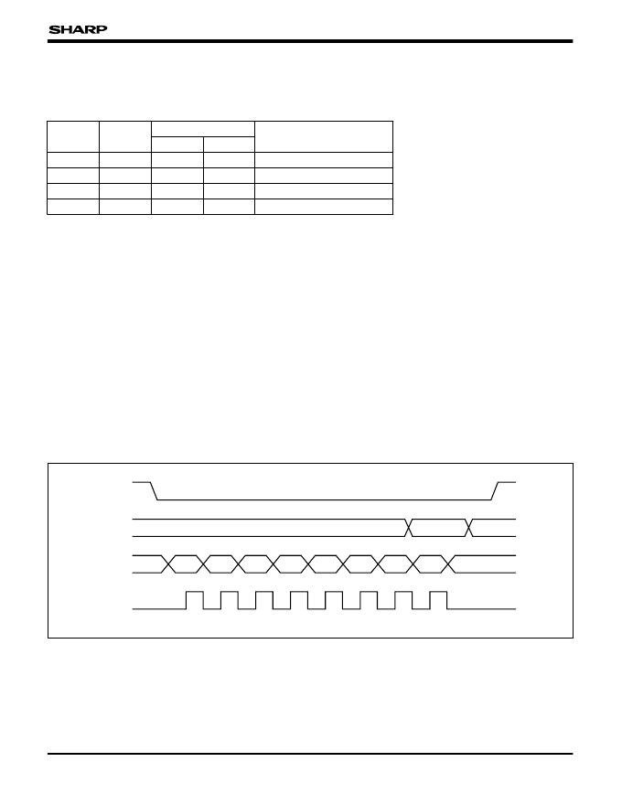
2.1.4. SERIAL INTERFACE
The serial interface of LH155BA can accept inputs
of SDA and SCL in the chip selection state (CSB =
"L"). When not in the chip selection state, the
internal shift register and counter are reset to their
initial condition.
Serial data SDA are input sequentially in order of
D
7
to D
0
at the rising edge of serial clock (SCL)
and are converted into 8-bit parallel data (by serial
to parallel conversion) at the rising edge of the 8th
serial clock, being processed in accordance with
the data. The identification whether the serial data
inputs (SDA) are display data or commands is
judged by input to RS pin.
RS = "L" : Display data
RS = "H" : Commands
After completing 8-bit data transferring, or when
making no access, be sure to set serial clock input
(SCL) to "L".
Protection of SDA and SCL signals against external
noise should be taken in actual wiring. To prevent
the successive recognition errors of transferring
data from external noise, release the chip selection
state (CSB = "H") at every completion of 8-bit data
transferring.
Valid
D
0
RS
SCL
SDA
CSB
D
1
D
2
D
3
D
4
D
5
D
6
D
7
8
7
6
5
4
3
2
1
相關(guān)PDF資料 |
PDF描述 |
|---|---|
| LH155R | Industrial Control IC |
| LH155P | Industrial Control IC |
| LH155N | Industrial Control IC |
| LH155L | Industrial Control IC |
| LH1554P | LCD Display Driver |
相關(guān)代理商/技術(shù)參數(shù) |
參數(shù)描述 |
|---|---|
| LH155L | 制造商:未知廠家 制造商全稱:未知廠家 功能描述:Industrial Control IC |
| LH155N | 制造商:未知廠家 制造商全稱:未知廠家 功能描述:Industrial Control IC |
| LH155P | 制造商:未知廠家 制造商全稱:未知廠家 功能描述:Industrial Control IC |
| LH155R | 制造商:未知廠家 制造商全稱:未知廠家 功能描述:Industrial Control IC |
| LH1560 | 制造商:未知廠家 制造商全稱:未知廠家 功能描述:LCD Display Driver |
發(fā)布緊急采購,3分鐘左右您將得到回復(fù)。