- 您現(xiàn)在的位置:買賣IC網(wǎng) > PDF目錄4594 > LFXP3E-3QN208I (Lattice Semiconductor Corporation)IC FPGA 3.1KLUTS 136I/O 208-PQFP PDF資料下載
參數(shù)資料
| 型號: | LFXP3E-3QN208I |
| 廠商: | Lattice Semiconductor Corporation |
| 文件頁數(shù): | 326/397頁 |
| 文件大小: | 0K |
| 描述: | IC FPGA 3.1KLUTS 136I/O 208-PQFP |
| 標(biāo)準(zhǔn)包裝: | 48 |
| 系列: | XP |
| 邏輯元件/單元數(shù): | 3000 |
| RAM 位總計(jì): | 55296 |
| 輸入/輸出數(shù): | 136 |
| 電源電壓: | 1.14 V ~ 1.26 V |
| 安裝類型: | 表面貼裝 |
| 工作溫度: | -40°C ~ 100°C |
| 封裝/外殼: | 208-BFQFP |
| 供應(yīng)商設(shè)備封裝: | 208-PQFP(28x28) |
第1頁第2頁第3頁第4頁第5頁第6頁第7頁第8頁第9頁第10頁第11頁第12頁第13頁第14頁第15頁第16頁第17頁第18頁第19頁第20頁第21頁第22頁第23頁第24頁第25頁第26頁第27頁第28頁第29頁第30頁第31頁第32頁第33頁第34頁第35頁第36頁第37頁第38頁第39頁第40頁第41頁第42頁第43頁第44頁第45頁第46頁第47頁第48頁第49頁第50頁第51頁第52頁第53頁第54頁第55頁第56頁第57頁第58頁第59頁第60頁第61頁第62頁第63頁第64頁第65頁第66頁第67頁第68頁第69頁第70頁第71頁第72頁第73頁第74頁第75頁第76頁第77頁第78頁第79頁第80頁第81頁第82頁第83頁第84頁第85頁第86頁第87頁第88頁第89頁第90頁第91頁第92頁第93頁第94頁第95頁第96頁第97頁第98頁第99頁第100頁第101頁第102頁第103頁第104頁第105頁第106頁第107頁第108頁第109頁第110頁第111頁第112頁第113頁第114頁第115頁第116頁第117頁第118頁第119頁第120頁第121頁第122頁第123頁第124頁第125頁第126頁第127頁第128頁第129頁第130頁第131頁第132頁第133頁第134頁第135頁第136頁第137頁第138頁第139頁第140頁第141頁第142頁第143頁第144頁第145頁第146頁第147頁第148頁第149頁第150頁第151頁第152頁第153頁第154頁第155頁第156頁第157頁第158頁第159頁第160頁第161頁第162頁第163頁第164頁第165頁第166頁第167頁第168頁第169頁第170頁第171頁第172頁第173頁第174頁第175頁第176頁第177頁第178頁第179頁第180頁第181頁第182頁第183頁第184頁第185頁第186頁第187頁第188頁第189頁第190頁第191頁第192頁第193頁第194頁第195頁第196頁第197頁第198頁第199頁第200頁第201頁第202頁第203頁第204頁第205頁第206頁第207頁第208頁第209頁第210頁第211頁第212頁第213頁第214頁第215頁第216頁第217頁第218頁第219頁第220頁第221頁第222頁第223頁第224頁第225頁第226頁第227頁第228頁第229頁第230頁第231頁第232頁第233頁第234頁第235頁第236頁第237頁第238頁第239頁第240頁第241頁第242頁第243頁第244頁第245頁第246頁第247頁第248頁第249頁第250頁第251頁第252頁第253頁第254頁第255頁第256頁第257頁第258頁第259頁第260頁第261頁第262頁第263頁第264頁第265頁第266頁第267頁第268頁第269頁第270頁第271頁第272頁第273頁第274頁第275頁第276頁第277頁第278頁第279頁第280頁第281頁第282頁第283頁第284頁第285頁第286頁第287頁第288頁第289頁第290頁第291頁第292頁第293頁第294頁第295頁第296頁第297頁第298頁第299頁第300頁第301頁第302頁第303頁第304頁第305頁第306頁第307頁第308頁第309頁第310頁第311頁第312頁第313頁第314頁第315頁第316頁第317頁第318頁第319頁第320頁第321頁第322頁第323頁第324頁第325頁當(dāng)前第326頁第327頁第328頁第329頁第330頁第331頁第332頁第333頁第334頁第335頁第336頁第337頁第338頁第339頁第340頁第341頁第342頁第343頁第344頁第345頁第346頁第347頁第348頁第349頁第350頁第351頁第352頁第353頁第354頁第355頁第356頁第357頁第358頁第359頁第360頁第361頁第362頁第363頁第364頁第365頁第366頁第367頁第368頁第369頁第370頁第371頁第372頁第373頁第374頁第375頁第376頁第377頁第378頁第379頁第380頁第381頁第382頁第383頁第384頁第385頁第386頁第387頁第388頁第389頁第390頁第391頁第392頁第393頁第394頁第395頁第396頁第397頁
PCB Layout Recommendations
Lattice Semiconductor
for BGA Packages
18-17
PCB cross-sectioning is another method used to verify BGA and PCB quality and reliability. After a new process
has been developed or changed or when qualifying a new vendor, it is a good practice to get physical information
from the vendor on their BGA reflow. When trace/space and drill or laser tolerances are nearing their limits, board
yield can be as be as low as 50% for the bare board fab. Cross-sections give you a good idea if the process is cor-
rect but do not guarantee each batch or each board design will behave the same way due to layout dimensions,
thermal issues, flux/paste and alignment, etc.
Figure 18-17. BGA Cross-Section
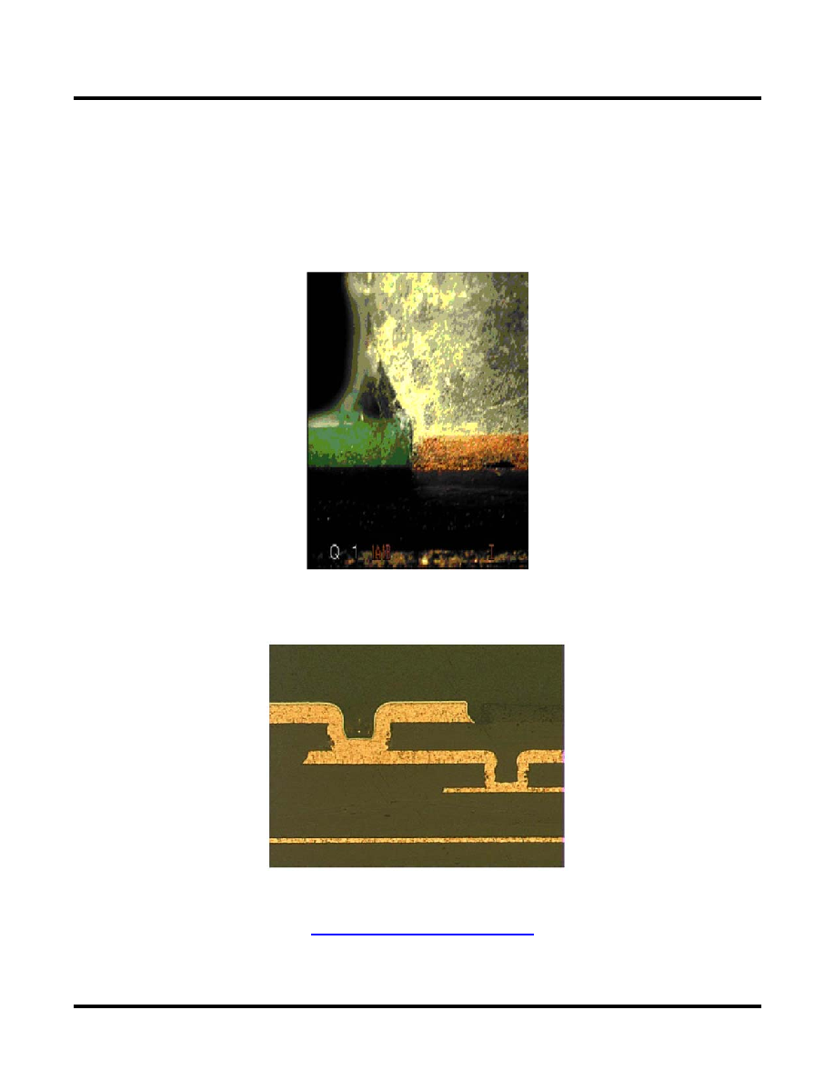
Figure 18-18 shows “offset” micro via stack routing between layers.
Figure 18-18. Cross-Section of Micro Vias
High-resolution video cameras are used for edge inspection to verify ball seating, distortion, solder wetting, flow,
contaminates, etc. Figure 18-19 is a video view of a side/edge shot looking at BGA balls soldered down to the isp-
MACH 4000ZE Pico Evaluation Board (www.latticesemi.com/4000ze-pico-kit), an FR4 4-layer PCB.
相關(guān)PDF資料 |
PDF描述 |
|---|---|
| LFXP3C-4QN208C | IC FPGA 3.1KLUTS 136I/O 208-PQFP |
| LFXP3C-3QN208I | IC FPGA 3.1KLUTS 136I/O 208-PQFP |
| MAX4925ELT+T | IC CTLR OVP W/EXT PFET 6UDFN |
| LFEC6E-3FN256C | IC FPGA 6.1KLUTS 195I/O 256-BGA |
| MAX4840EXT+T | IC CTLR OVP 5.8V SC70-6 |
相關(guān)代理商/技術(shù)參數(shù) |
參數(shù)描述 |
|---|---|
| LFXP3E-3T100C | 功能描述:FPGA - 現(xiàn)場可編程門陣列 3.1K LUTs 62 IO 1.2V -3 Spd RoHS:否 制造商:Altera Corporation 系列:Cyclone V E 柵極數(shù)量: 邏輯塊數(shù)量:943 內(nèi)嵌式塊RAM - EBR:1956 kbit 輸入/輸出端數(shù)量:128 最大工作頻率:800 MHz 工作電源電壓:1.1 V 最大工作溫度:+ 70 C 安裝風(fēng)格:SMD/SMT 封裝 / 箱體:FBGA-256 |
| LFXP3E-3T100I | 功能描述:FPGA - 現(xiàn)場可編程門陣列 3.1K LUTs 62 IO 1.2V -3 Spd I RoHS:否 制造商:Altera Corporation 系列:Cyclone V E 柵極數(shù)量: 邏輯塊數(shù)量:943 內(nèi)嵌式塊RAM - EBR:1956 kbit 輸入/輸出端數(shù)量:128 最大工作頻率:800 MHz 工作電源電壓:1.1 V 最大工作溫度:+ 70 C 安裝風(fēng)格:SMD/SMT 封裝 / 箱體:FBGA-256 |
| LFXP3E-3T144C | 功能描述:FPGA - 現(xiàn)場可編程門陣列 3.1K LUTs 100 IO 1.2 V -3 Spd RoHS:否 制造商:Altera Corporation 系列:Cyclone V E 柵極數(shù)量: 邏輯塊數(shù)量:943 內(nèi)嵌式塊RAM - EBR:1956 kbit 輸入/輸出端數(shù)量:128 最大工作頻率:800 MHz 工作電源電壓:1.1 V 最大工作溫度:+ 70 C 安裝風(fēng)格:SMD/SMT 封裝 / 箱體:FBGA-256 |
| LFXP3E-3T144I | 功能描述:FPGA - 現(xiàn)場可編程門陣列 3.1K LUTs 100 IO 1.2 V -3 Spd I RoHS:否 制造商:Altera Corporation 系列:Cyclone V E 柵極數(shù)量: 邏輯塊數(shù)量:943 內(nèi)嵌式塊RAM - EBR:1956 kbit 輸入/輸出端數(shù)量:128 最大工作頻率:800 MHz 工作電源電壓:1.1 V 最大工作溫度:+ 70 C 安裝風(fēng)格:SMD/SMT 封裝 / 箱體:FBGA-256 |
| LFXP3E-3TN100C | 功能描述:FPGA - 現(xiàn)場可編程門陣列 3.1K LUTs 62 IO 1.2V -3 Spd RoHS:否 制造商:Altera Corporation 系列:Cyclone V E 柵極數(shù)量: 邏輯塊數(shù)量:943 內(nèi)嵌式塊RAM - EBR:1956 kbit 輸入/輸出端數(shù)量:128 最大工作頻率:800 MHz 工作電源電壓:1.1 V 最大工作溫度:+ 70 C 安裝風(fēng)格:SMD/SMT 封裝 / 箱體:FBGA-256 |
發(fā)布緊急采購,3分鐘左右您將得到回復(fù)。