- 您現(xiàn)在的位置:買賣IC網(wǎng) > PDF目錄299403 > LFSC3GA15E-6FN256I (LATTICE SEMICONDUCTOR CORP) PDF資料下載
參數(shù)資料
| 型號(hào): | LFSC3GA15E-6FN256I |
| 廠商: | LATTICE SEMICONDUCTOR CORP |
| 元件分類: | FPGA |
| 中文描述: | FPGA, 56 CLBS, 15000 GATES, 1000 MHz, PBGA256 |
| 封裝: | 17 X 17 MM, LEAD FREE, FPBGA-256 |
| 文件頁(yè)數(shù): | 220/243頁(yè) |
| 文件大?。?/td> | 2674K |
| 代理商: | LFSC3GA15E-6FN256I |
第1頁(yè)第2頁(yè)第3頁(yè)第4頁(yè)第5頁(yè)第6頁(yè)第7頁(yè)第8頁(yè)第9頁(yè)第10頁(yè)第11頁(yè)第12頁(yè)第13頁(yè)第14頁(yè)第15頁(yè)第16頁(yè)第17頁(yè)第18頁(yè)第19頁(yè)第20頁(yè)第21頁(yè)第22頁(yè)第23頁(yè)第24頁(yè)第25頁(yè)第26頁(yè)第27頁(yè)第28頁(yè)第29頁(yè)第30頁(yè)第31頁(yè)第32頁(yè)第33頁(yè)第34頁(yè)第35頁(yè)第36頁(yè)第37頁(yè)第38頁(yè)第39頁(yè)第40頁(yè)第41頁(yè)第42頁(yè)第43頁(yè)第44頁(yè)第45頁(yè)第46頁(yè)第47頁(yè)第48頁(yè)第49頁(yè)第50頁(yè)第51頁(yè)第52頁(yè)第53頁(yè)第54頁(yè)第55頁(yè)第56頁(yè)第57頁(yè)第58頁(yè)第59頁(yè)第60頁(yè)第61頁(yè)第62頁(yè)第63頁(yè)第64頁(yè)第65頁(yè)第66頁(yè)第67頁(yè)第68頁(yè)第69頁(yè)第70頁(yè)第71頁(yè)第72頁(yè)第73頁(yè)第74頁(yè)第75頁(yè)第76頁(yè)第77頁(yè)第78頁(yè)第79頁(yè)第80頁(yè)第81頁(yè)第82頁(yè)第83頁(yè)第84頁(yè)第85頁(yè)第86頁(yè)第87頁(yè)第88頁(yè)第89頁(yè)第90頁(yè)第91頁(yè)第92頁(yè)第93頁(yè)第94頁(yè)第95頁(yè)第96頁(yè)第97頁(yè)第98頁(yè)第99頁(yè)第100頁(yè)第101頁(yè)第102頁(yè)第103頁(yè)第104頁(yè)第105頁(yè)第106頁(yè)第107頁(yè)第108頁(yè)第109頁(yè)第110頁(yè)第111頁(yè)第112頁(yè)第113頁(yè)第114頁(yè)第115頁(yè)第116頁(yè)第117頁(yè)第118頁(yè)第119頁(yè)第120頁(yè)第121頁(yè)第122頁(yè)第123頁(yè)第124頁(yè)第125頁(yè)第126頁(yè)第127頁(yè)第128頁(yè)第129頁(yè)第130頁(yè)第131頁(yè)第132頁(yè)第133頁(yè)第134頁(yè)第135頁(yè)第136頁(yè)第137頁(yè)第138頁(yè)第139頁(yè)第140頁(yè)第141頁(yè)第142頁(yè)第143頁(yè)第144頁(yè)第145頁(yè)第146頁(yè)第147頁(yè)第148頁(yè)第149頁(yè)第150頁(yè)第151頁(yè)第152頁(yè)第153頁(yè)第154頁(yè)第155頁(yè)第156頁(yè)第157頁(yè)第158頁(yè)第159頁(yè)第160頁(yè)第161頁(yè)第162頁(yè)第163頁(yè)第164頁(yè)第165頁(yè)第166頁(yè)第167頁(yè)第168頁(yè)第169頁(yè)第170頁(yè)第171頁(yè)第172頁(yè)第173頁(yè)第174頁(yè)第175頁(yè)第176頁(yè)第177頁(yè)第178頁(yè)第179頁(yè)第180頁(yè)第181頁(yè)第182頁(yè)第183頁(yè)第184頁(yè)第185頁(yè)第186頁(yè)第187頁(yè)第188頁(yè)第189頁(yè)第190頁(yè)第191頁(yè)第192頁(yè)第193頁(yè)第194頁(yè)第195頁(yè)第196頁(yè)第197頁(yè)第198頁(yè)第199頁(yè)第200頁(yè)第201頁(yè)第202頁(yè)第203頁(yè)第204頁(yè)第205頁(yè)第206頁(yè)第207頁(yè)第208頁(yè)第209頁(yè)第210頁(yè)第211頁(yè)第212頁(yè)第213頁(yè)第214頁(yè)第215頁(yè)第216頁(yè)第217頁(yè)第218頁(yè)第219頁(yè)當(dāng)前第220頁(yè)第221頁(yè)第222頁(yè)第223頁(yè)第224頁(yè)第225頁(yè)第226頁(yè)第227頁(yè)第228頁(yè)第229頁(yè)第230頁(yè)第231頁(yè)第232頁(yè)第233頁(yè)第234頁(yè)第235頁(yè)第236頁(yè)第237頁(yè)第238頁(yè)第239頁(yè)第240頁(yè)第241頁(yè)第242頁(yè)第243頁(yè)
4-4
Pinout Information
Lattice Semiconductor
LatticeSC/M Family Data Sheet
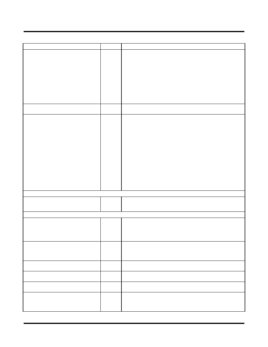
D[n:0]
I/O
In parallel configuration modes, D[7:0] receives configuration data,
and each pin is pull-up enabled. For slave serial mode, D0 is the data
input.
D[7:3] is the output internal status for peripheral mode when RDN is
low.
D[7:0] is also the first byte of MPI data pins.
In MPI configuration mode, MPI selectable data bus width from 8 and
16-bit. Driven by a bus master in a write transaction. Driven by MPI in
a read transaction.
DP[m:0]
I/O
MPI selectable parity data bus width from 1, 2, and 3-bit DP[0] for
D[7:0], DP[1] for D[15:8], and DP[2] for D[23:16].
BUSYN/RCLK/SCK
O
During configuration in peripheral mode, high on BUSYN indicates
another byte can be written to the FPGA. If a read operation is done
when the device is selected, the same status is also available on D[7]
in asynchronous peripheral mode.
During configuration in slave parallel mode, low on BUSYN inhibits the
external host from sending new data. The output is used by slave par-
allel and master serial modes only for decompression.
During configuration in master parallel and master byte modes, RCLK
is a read clock output signal to an external memory. The RCLK fre-
quency is the same as CCLK when used with uncompressed bit-
streams. RCLK will be 1/8 the frequency of CCLK when the bitstream
is compressed.
During configuration in SPI modes, SCK is generated by the device
and connected to the CLK input of the FLASH memory.
MPI Interface (Dedicated pin)
MPI_IRQ_N
O
MPI Interrupt request active low signal is controlled by system bus
interrupt controller and may be sourced from any bus error or MPI con-
figuration error. It can be connected to one of MPC860 IRQ pins.
MPI Interface (User I/O if MPI is not used.)
MPI_CS0N MPI_CS1
I
MPI chip select pins, active low on MPI_CS0N while active high on
MPI_CS1. Both have to be active during the whole transfer data
phase. During transfer address phase, both can be inactive so that the
decoding for them from address can be slow. If they are active during
address phase, one cycle can be saved for sync read.
MPI_CLK
I
This is the PowerPC bus clock. It can be a source of the clock for
embedded system bus. If MPI_CLK is used as system bus clock, MPI
will be set into sync mode by default. All of the operation on PowerPC
side of MPI are synchronized to the rising edge of this clock.
MPI_TSIZ[1:0]
I
Driven by a bus master to indicate the data transfer size for the trans-
action. 01 for byte, 10 for half-word, and 00 for word.
MPI_WR_N
I
Driven high indicates that a read access is in progress. Driven low
indicates that a write access is in process.
MPI_BURST
I
Driven active low indicates that a burst transfer is in progress. Driven
high indicates that the current transfer is not a burst.
MPI_BDIP
I
Active low “Burst Data in Process” is driven by a PowerPC processor.
Asserted indicates that the second beat in front of the current one is
requested by the master. Negated before the burst transfer ends to
abort the burst data phase.
Signal Descriptions (Cont.)
Signal Name
I/O
Description
相關(guān)PDF資料 |
PDF描述 |
|---|---|
| LFSCM3GA40EP1-5FFN1020I | |
| LFXP2-40E-6FN484I | |
| LFXP2-17E-7F484C | |
| LFXP20E-3FN484C | |
| LFXP20E-5FN484C | |
相關(guān)代理商/技術(shù)參數(shù) |
參數(shù)描述 |
|---|---|
| LFSC3GA15E-6FN900C | 功能描述:FPGA - 現(xiàn)場(chǎng)可編程門陣列 15.2K LUTs 3G SERDES 1.2V -6 Spd RoHS:否 制造商:Altera Corporation 系列:Cyclone V E 柵極數(shù)量: 邏輯塊數(shù)量:943 內(nèi)嵌式塊RAM - EBR:1956 kbit 輸入/輸出端數(shù)量:128 最大工作頻率:800 MHz 工作電源電壓:1.1 V 最大工作溫度:+ 70 C 安裝風(fēng)格:SMD/SMT 封裝 / 箱體:FBGA-256 |
| LFSC3GA15E-6FN900I | 功能描述:FPGA - 現(xiàn)場(chǎng)可編程門陣列 15.2K LUTs 3G SERDES 1.2V -6 Spd I RoHS:否 制造商:Altera Corporation 系列:Cyclone V E 柵極數(shù)量: 邏輯塊數(shù)量:943 內(nèi)嵌式塊RAM - EBR:1956 kbit 輸入/輸出端數(shù)量:128 最大工作頻率:800 MHz 工作電源電壓:1.1 V 最大工作溫度:+ 70 C 安裝風(fēng)格:SMD/SMT 封裝 / 箱體:FBGA-256 |
| LFSC3GA15E-7F256C | 功能描述:FPGA - 現(xiàn)場(chǎng)可編程門陣列 15.2K LUTs 3G SERDES 1.2V -7 Spd RoHS:否 制造商:Altera Corporation 系列:Cyclone V E 柵極數(shù)量: 邏輯塊數(shù)量:943 內(nèi)嵌式塊RAM - EBR:1956 kbit 輸入/輸出端數(shù)量:128 最大工作頻率:800 MHz 工作電源電壓:1.1 V 最大工作溫度:+ 70 C 安裝風(fēng)格:SMD/SMT 封裝 / 箱體:FBGA-256 |
| LFSC3GA15E-7F900C | 功能描述:FPGA - 現(xiàn)場(chǎng)可編程門陣列 15.2K LUTs 3G SERDES 1.2V -7 Spd RoHS:否 制造商:Altera Corporation 系列:Cyclone V E 柵極數(shù)量: 邏輯塊數(shù)量:943 內(nèi)嵌式塊RAM - EBR:1956 kbit 輸入/輸出端數(shù)量:128 最大工作頻率:800 MHz 工作電源電壓:1.1 V 最大工作溫度:+ 70 C 安裝風(fēng)格:SMD/SMT 封裝 / 箱體:FBGA-256 |
| LFSC3GA15E-7FN256C | 功能描述:FPGA - 現(xiàn)場(chǎng)可編程門陣列 15.2K LUTs 3G SERDES 1.2V -7 Spd RoHS:否 制造商:Altera Corporation 系列:Cyclone V E 柵極數(shù)量: 邏輯塊數(shù)量:943 內(nèi)嵌式塊RAM - EBR:1956 kbit 輸入/輸出端數(shù)量:128 最大工作頻率:800 MHz 工作電源電壓:1.1 V 最大工作溫度:+ 70 C 安裝風(fēng)格:SMD/SMT 封裝 / 箱體:FBGA-256 |
發(fā)布緊急采購(gòu),3分鐘左右您將得到回復(fù)。