- 您現(xiàn)在的位置:買賣IC網(wǎng) > PDF目錄30737 > LC89517K SPECIALTY CONSUMER CIRCUIT, PQFP100 PDF資料下載
參數(shù)資料
| 型號(hào): | LC89517K |
| 元件分類: | 消費(fèi)家電 |
| 英文描述: | SPECIALTY CONSUMER CIRCUIT, PQFP100 |
| 封裝: | QFP-100 |
| 文件頁(yè)數(shù): | 1/6頁(yè) |
| 文件大小: | 180K |
| 代理商: | LC89517K |

Ordering number : EN*4854A
12395TH (OT) No. 4854-1/6
Overview
The LC89517K is a CD-ROM/CD-I error correction LSI
that integrates the functions provided by the improved
version of the LC89515 and a sub-code function in a
single chip. The improved version of the LC89515
additionally supports double speed operation.
Features
Support for double speed operation (selectable by setting
an internal register) at an operating frequency of
16.9344 MHz
Built-in 12-byte FIFO for transfers from the system
microcontroller to the host computer
Built-in 12-byte FIFO for transfers from the host
computer to the system microcontroller
Direct connection to the LC8955 (an ADPCM decoder
LSI) and the LC8953 (a 68000 CPU peripheral interface
LSI)
Sub-code data can be written to buffer RAM simply by
connecting the CD DSP sub-code pin. This allows the
system microcontroller to read the sub-code values.
The system microcontroller can access buffer RAM
through the LC89517K.
Pseudo-SRAM support (An interface circuit is built in.)
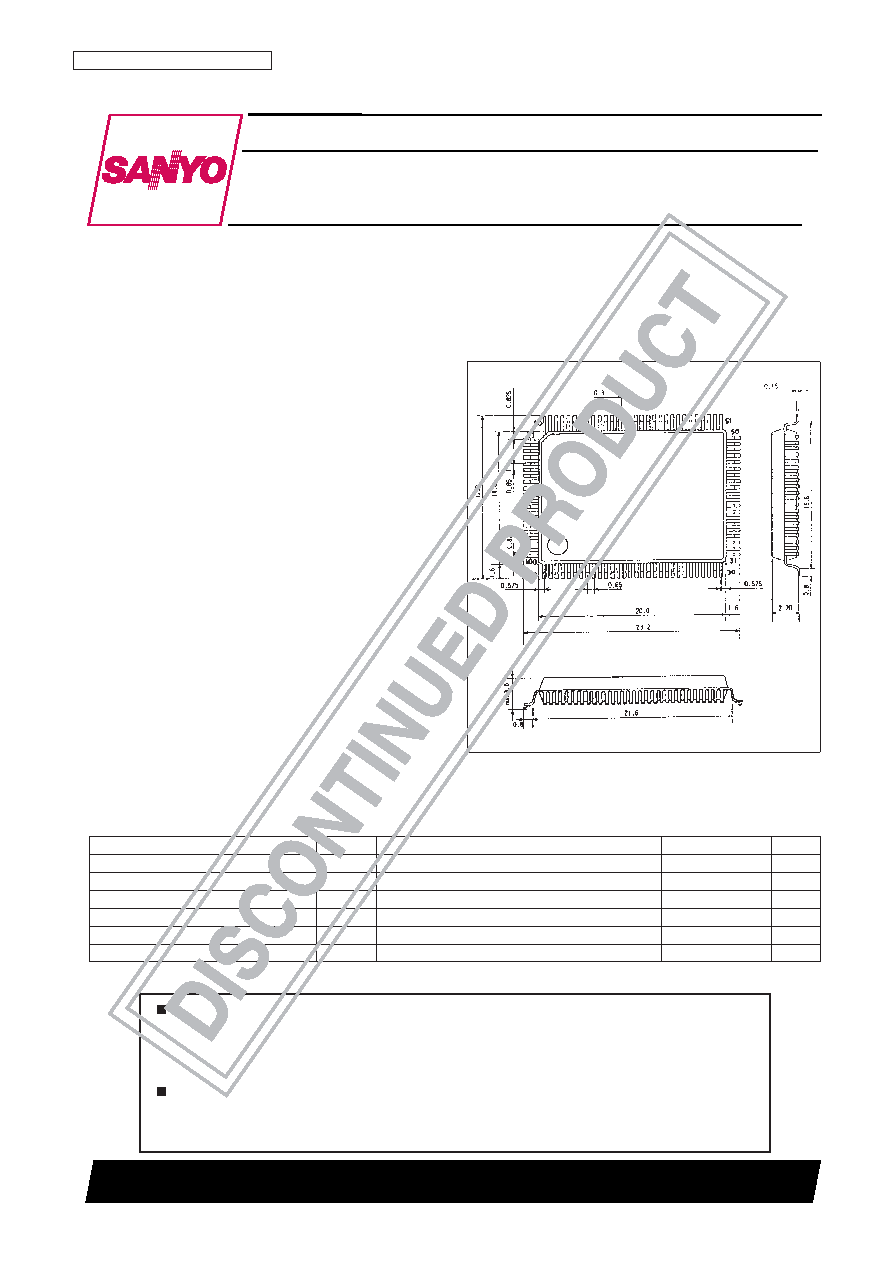
Package Dimensions
unit: mm
3151-QFP100E (FLP100)
Preliminary
SANYO: QIP100E (FLP100)
[LC89517K]
LC89517K
SANYO Electric Co.,Ltd. Semiconductor Bussiness Headquarters
TOKYO OFFICE Tokyo Bldg., 1-10, 1 Chome, Ueno, Taito-ku, TOKYO, 110-8534 JAPAN
Built-in Subcode Interface CD-ROM/CD-I Error
Correction LSI
CMOS LSI
Any and all SANYO products described or contained herein do not have specifications that can handle
applications that require extremely high levels of reliability, such as life-support systems, aircraft’s
control systems, or other applications whose failure can be reasonably expected to result in serious
physical and/or material damage. Consult with your SANYO representative nearest you before using
any SANYO products described or contained herein in such applications.
SANYO assumes no responsibility for equipment failures that result from using products at values that
exceed, even momentarily, rated values (such as maximum ratings, operating condition ranges, or other
parameters) listed in products specifications of any and all SANYO products described or contained
herein.
Specifications
Absolute Maximum Ratings at VSS = 0 V
Parameter
Symbol
Conditions
Ratings
Unit
Maximum supply voltage
VDD max
Ta = 25°C
–0.3 to +7.0
V
I/O voltage
VI, VO
Ta = 25°C
–0.3 to VDD + 0.3
V
Allowable power dissipation
Pd max
Ta ≤ 70°C
350
mW
Operating temperature
Topr
–30 to +70
°C
Storage temperature
Tstg
–55 to +125
°C
Soldering temperature
10 seconds
260
°C
相關(guān)PDF資料 |
PDF描述 |
|---|---|
| LC895194 | SPECIALTY CONSUMER CIRCUIT, PQFP144 |
| LC895195 | SPECIALTY CONSUMER CIRCUIT, PQFP144 |
| LC895196K | SPECIALTY CONSUMER CIRCUIT, PQFP144 |
| LC895196 | SPECIALTY CONSUMER CIRCUIT, PQFP144 |
| LC895198 | SPECIALTY CONSUMER CIRCUIT, PQFP120 |
相關(guān)代理商/技術(shù)參數(shù) |
參數(shù)描述 |
|---|---|
| LC895194 | 制造商:SANYO 制造商全稱:Sanyo Semicon Device 功能描述:CD-ROM Error Correction LSI with On-Chip ATA-PI (IDE) Interface |
| LC895195 | 制造商:SANYO 制造商全稱:Sanyo Semicon Device 功能描述:ATA-PI (IDE) CD-ROM Decoder LSI |
| LC895196 | 制造商:SANYO 制造商全稱:Sanyo Semicon Device 功能描述:ATA-PI Compatible CD-ROM Decoder IC |
| LC895196K | 制造商:SANYO 制造商全稱:Sanyo Semicon Device 功能描述:ATA-PI Compatible CD-ROM Decoder IC |
| LC895198 | 制造商:SANYO 制造商全稱:Sanyo Semicon Device 功能描述:CD-ROM Decoder for 32 x ATAPI (IDE) Drives |
發(fā)布緊急采購(gòu),3分鐘左右您將得到回復(fù)。