- 您現(xiàn)在的位置:買賣IC網(wǎng) > PDF目錄358765 > LC78621E (Sanyo Electric Co.,Ltd.) Compact Disc Player DSP(用于CD播放器的8位DSP) PDF資料下載
參數(shù)資料
| 型號: | LC78621E |
| 廠商: | Sanyo Electric Co.,Ltd. |
| 英文描述: | Compact Disc Player DSP(用于CD播放器的8位DSP) |
| 中文描述: | 光碟機的DSP(用于光盤播放器的8位數(shù)字信號處理器) |
| 文件頁數(shù): | 8/34頁 |
| 文件大小: | 417K |
| 代理商: | LC78621E |
第1頁第2頁第3頁第4頁第5頁第6頁第7頁當(dāng)前第8頁第9頁第10頁第11頁第12頁第13頁第14頁第15頁第16頁第17頁第18頁第19頁第20頁第21頁第22頁第23頁第24頁第25頁第26頁第27頁第28頁第29頁第30頁第31頁第32頁第33頁第34頁
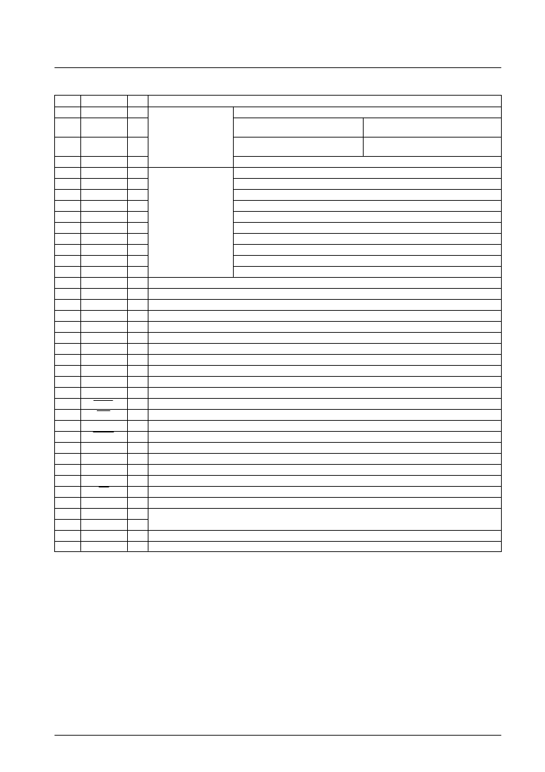
Continued from preceding page.
No. 5223-8/34
LC78621E
Pin No.
Symbol
I/O
Function
42
LRSY
O
Left/right clock output
43
CK2
O
Bit clock output
(after reset)
Inverted polarity clock output
(during CK2CON mode)
ROMXA application
output signals
44
ROMXA
O
Interpolation data output
(after reset)
ROM data output
(During ROMXA mode)
45
C2F
O
C2 flag output
46
MUTEL
O
Left channel mute output
47
LV
DD
LCHP
Left channel power supply.
48
O
Left channel P output
49
LCHN
O
Left channel N output
50
LV
SS
RV
SS
RCHN
One-bit D/A converter
Left channel ground. Normally 0 V.
51
Right channel ground. Normally 0 V.
52
O
Right channel N output
53
RCHP
O
Right channel P output
54
RV
DD
MUTER
Right channel power supply.
55
O
Right channel mute output
56
DOUT
O
Digital output
57
SBSY
O
Subcode block synchronization signal
58
EFLG
O
C1, C2, single and double error correction monitor pin
59
PW
O
Subcode P, Q, R, S, T, U, V and W output
60
SFSY
O
Subcode frame synchronization signal output. This signal falls when the subcodes are in the standby state.
61
SBCK
I
Subcode readout clock input. This is a Schmitt input. (Must be tied low when unused.)
62
FSX
O
Output for the 7.35 kHz synchronization signal divided from the crystal oscillator
63
WRQ
O
Subcode Q output standby output
64
RWC
I
Read/write control input. This is a Schmitt input.
65
SQOUT
O
Subcode Q output
66
COIN
I
Command input from the control microprocessor
67
CQCK
I
Input for both the command input acquisition clock and the SQOUT pin subcode readout clock input. This is a Schmitt input.
68
RES
I
Chip reset input. This pin must be set low briefly after power is first applied.
69
TST11
O
Test output. Leave open. (Normally outputs a low level.)
70
LASER
O
Laser on/off output. Controlled by serial data commands from the control microprocessor.
71
16M
O
16.9344 MHz output.
72
4.2M
O
4.2336 MHz output
73
CONT
O
Supplementary control output. Controlled by serial data commands from the control microprocessor.
74
TEST5
I
Test input. A pull-down resistor is built in.
75
CS
I
Chip select input. A pull-down resistor is built in.
76
XV
SS
X
IN
X
OUT
XV
DD
TEST1
Crystal oscillator ground. Normally 0 V.
77
I
Connections for a 16.9344 MHz crystal oscillator.
78
O
79
Crystal oscillator power supply.
80
I
Test input. A pull-down resistor is built in.
相關(guān)PDF資料 |
PDF描述 |
|---|---|
| LC78622E | Compact Disc Player DSP(用于CD播放器的8位DSP) |
| LC78622NE | Compact Disc Player DSP(用于CD播放器的8位DSP) |
| LC78624E | Compact Disc Player DSP(用于CD播放器的8位DSP) |
| LC78625E | SigmaDSP 28-/56-Bit Audio Processor with Two ADCs and Four DACs |
| LC78625 | SigmaDSP 28-/56-Bit Audio Processor with Two ADCs and Four DACs |
相關(guān)代理商/技術(shù)參數(shù) |
參數(shù)描述 |
|---|---|
| LC78622E | 制造商:SANYO 制造商全稱:Sanyo Semicon Device 功能描述:Compact Disc Player DSP |
| LC78622NE | 制造商:SANYO 制造商全稱:Sanyo Semicon Device 功能描述:Compact Disc Player DSP |
| LC78624E | 制造商:SANYO 制造商全稱:Sanyo Semicon Device 功能描述:Compact Disc Player DSP |
| LC78625 | 制造商:SANYO 制造商全稱:Sanyo Semicon Device 功能描述:Compact Disc Player DSP |
| LC78625E | 制造商:SANYO 制造商全稱:Sanyo Semicon Device 功能描述:Compact Disc Player DSP |
發(fā)布緊急采購,3分鐘左右您將得到回復(fù)。