- 您現(xiàn)在的位置:買賣IC網(wǎng) > PDF目錄19583 > LC51024VG-75F484I (Lattice Semiconductor Corporation)IC XPLD 1024MC 7.5NS 484FPBGA PDF資料下載
參數(shù)資料
| 型號: | LC51024VG-75F484I |
| 廠商: | Lattice Semiconductor Corporation |
| 文件頁數(shù): | 10/99頁 |
| 文件大小: | 0K |
| 描述: | IC XPLD 1024MC 7.5NS 484FPBGA |
| 標(biāo)準(zhǔn)包裝: | 60 |
| 系列: | ispMACH™ 5000VG |
| 可編程類型: | 系統(tǒng)內(nèi)可編程 |
| 最大延遲時間 tpd(1): | 7.5ns |
| 電壓電源 - 內(nèi)部: | 3 V ~ 3.6 V |
| 邏輯元件/邏輯塊數(shù)目: | 32 |
| 宏單元數(shù): | 1024 |
| 輸入/輸出數(shù): | 304 |
| 工作溫度: | -40°C ~ 105°C |
| 安裝類型: | 表面貼裝 |
| 封裝/外殼: | 484-BBGA |
| 供應(yīng)商設(shè)備封裝: | 484-FPBGA(23x23) |
| 包裝: | 托盤 |
第1頁第2頁第3頁第4頁第5頁第6頁第7頁第8頁第9頁當(dāng)前第10頁第11頁第12頁第13頁第14頁第15頁第16頁第17頁第18頁第19頁第20頁第21頁第22頁第23頁第24頁第25頁第26頁第27頁第28頁第29頁第30頁第31頁第32頁第33頁第34頁第35頁第36頁第37頁第38頁第39頁第40頁第41頁第42頁第43頁第44頁第45頁第46頁第47頁第48頁第49頁第50頁第51頁第52頁第53頁第54頁第55頁第56頁第57頁第58頁第59頁第60頁第61頁第62頁第63頁第64頁第65頁第66頁第67頁第68頁第69頁第70頁第71頁第72頁第73頁第74頁第75頁第76頁第77頁第78頁第79頁第80頁第81頁第82頁第83頁第84頁第85頁第86頁第87頁第88頁第89頁第90頁第91頁第92頁第93頁第94頁第95頁第96頁第97頁第98頁第99頁
Lattice Semiconductor
ispXPLD 5000MX Family Data Sheet
14
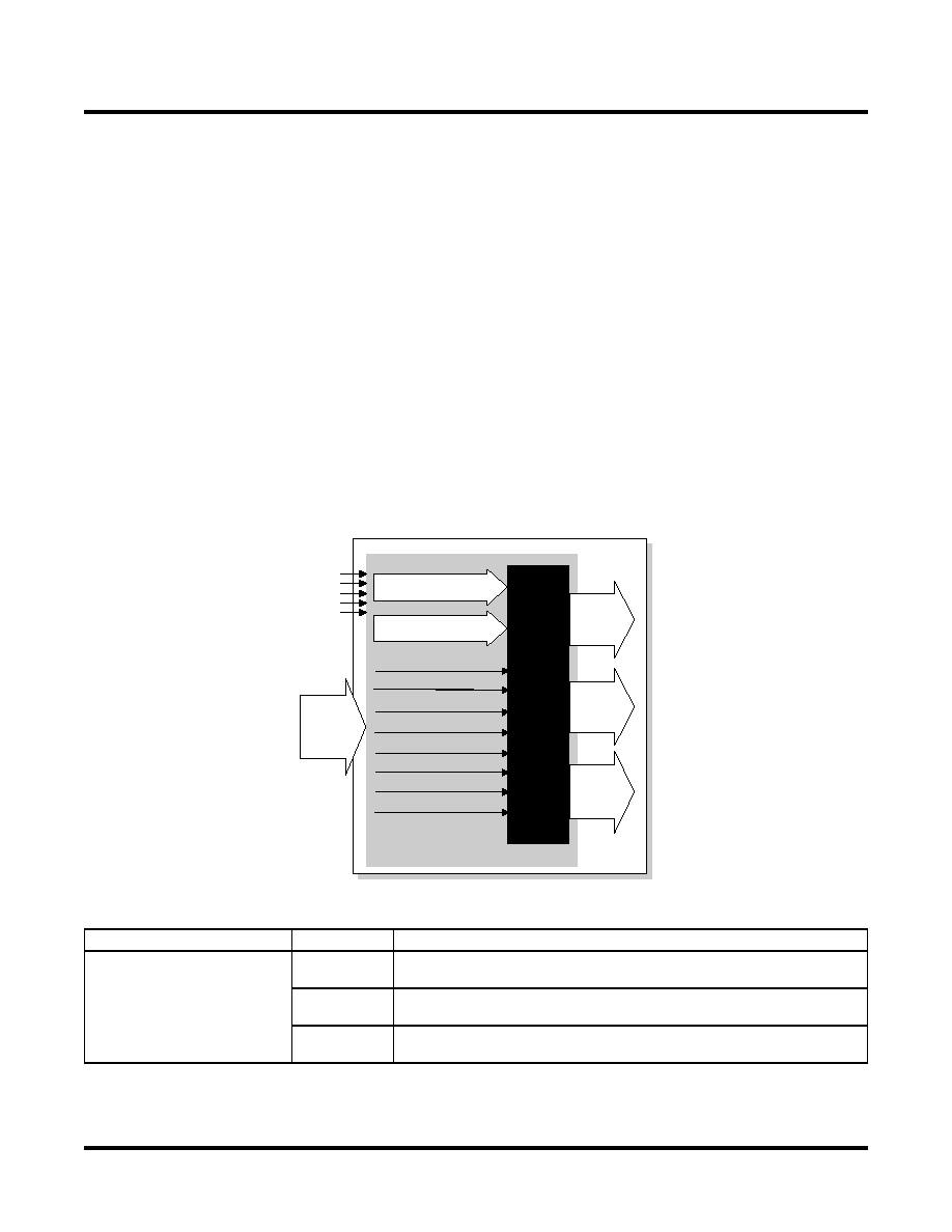
CAM Mode
In CAM Mode the multi-function array is configured as a Ternary Content Addressable Memory (CAM). CAM
behaves like a reverse memory where the input is data and the output is an address. It can be used to perform a
variety of high-performance look-up functions. As such, CAM has two modes of operation. In write or update mode
the CAM behaves as a RAM and data is written to the supplied address. In read or compare operations data is sup-
plied to the CAM and if this matches any of the data in the array the Match and Multiple Match (if there is more than
one match) flags are set to true and the lowest address with matching data is output. The CAM contains 128
entries of 48 bits. Figure 13 shows the block diagram of the CAM.
To further enhance the flexibility of the CAM a mask register is available. If enabled during updates, bits corre-
sponding with those set to 1 in the mask register are not updated. If enabled during compare operations, bits corre-
sponding to those set to 1 in the mask register are not included in the compare. A write don’t care signal allows
don’t cares to be programmed into the CAM if desired. Like other write operations the mask register controls this.
The write/comp data, write address, write enable, write chip select, and write don’t care signals are synchronous.
The CAM Output signals, match flag, and multimatch flag can be synchronous or asynchronous. The Enable mask
register input is not latched but must meet setup and hold times relative to the write clock. All inputs must use the
same clock and clock enable signals. All outputs must use the same clock and clock enable signals. Reset is com-
mon for both inputs and outputs. Table 9 shows the allowable sources for clock, clock enable, and reset for the var-
ious CAM registers.
Figure 13. CAM Mode
Table 9. Register Clocks, Clock Enables, and Initialization in CAM Mode
Register
Input
Source
Write data, Write address,
Enable mask register, Write
enable, write chip select, and
write don’t care, CAM Output,
Match, and Multimatch
Clock
CLK or one of the global clocks (CLK0 - CLK3). Each of these signals can
be inverted if required.
Clock Enable
WE or one of the global clocks (CLK1 - CLK 2). Each of these signals can
be inverted if required.
Reset
Created by the logical OR of the global reset signal and RST. RST is routed
by the multifunction array from GRP, with inversion if desired
‘
68 Inputs
From
Routing
Write Enable (WE)
En Mask Reg (EN_MASK)
Reset (RST)
Write Chip Sel (WCS[0:1])
CLK (CLK)
Clock Enable (CE)
Write/Comp Data
(WD[0:31])
128X48
CAM
Write Address
(WAD[0:6])
WR Mask Reg (WR_MASK)
WR don t care (WR_DC)
RESET
CLK0
CLK3
CLK1
CLK2
CAM
Output
CO[0:6]
Match
Out
MATCH
Multi-
match
Out
MUL_MATCH
SELECT
DEVICES
DISCONTINUED
相關(guān)PDF資料 |
PDF描述 |
|---|---|
| EPM7032STI44-7N | IC MAX 7000 CPLD 32 44-TQFP |
| AGM22DRST-S664 | CONN EDGECARD 44POS DIP .156 SLD |
| MIC5256-2.85BM5 TR | IC REG LDO 2.85V .15A SOT23-5 |
| V375A3V3E264BF | CONVERTER MOD DC/DC 3.3V 264W |
| V375A3V3E264BL3 | CONVERTER MOD DC/DC 3.3V 264W |
相關(guān)代理商/技術(shù)參數(shù) |
參數(shù)描述 |
|---|---|
| LC51024VG-75F676C | 功能描述:CPLD - 復(fù)雜可編程邏輯器件 PROGRAM EXPANDED LOG RoHS:否 制造商:Lattice 系列: 存儲類型:EEPROM 大電池數(shù)量:128 最大工作頻率:333 MHz 延遲時間:2.7 ns 可編程輸入/輸出端數(shù)量:64 工作電源電壓:3.3 V 最大工作溫度:+ 90 C 最小工作溫度:0 C 封裝 / 箱體:TQFP-100 |
| LC51024VG-75F676I | 功能描述:CPLD - 復(fù)雜可編程邏輯器件 PROGRAM EXPANDED LOG RoHS:否 制造商:Lattice 系列: 存儲類型:EEPROM 大電池數(shù)量:128 最大工作頻率:333 MHz 延遲時間:2.7 ns 可編程輸入/輸出端數(shù)量:64 工作電源電壓:3.3 V 最大工作溫度:+ 90 C 最小工作溫度:0 C 封裝 / 箱體:TQFP-100 |
| LC511 | 制造商:SEOUL 制造商全稱:Seoul Semiconductor 功能描述:RED OVAL LAMP LED |
| LC511-200/N | 制造商:Newport Electronics Inc 功能描述:SENSOR, LOAD CELL, 200LB, 3MV/V, Load Capacity:200lb, Cell Output mV / V:3, External Depth:25mm, Length:121mm, Operating Temperature Min:-34C, Operating Temperature Max:82C, Supply Voltage:15VDC , RoHS Compliant: Yes |
| LC5128B-10T128I | 功能描述:CPLD - 復(fù)雜可編程邏輯器件 RoHS:否 制造商:Lattice 系列: 存儲類型:EEPROM 大電池數(shù)量:128 最大工作頻率:333 MHz 延遲時間:2.7 ns 可編程輸入/輸出端數(shù)量:64 工作電源電壓:3.3 V 最大工作溫度:+ 90 C 最小工作溫度:0 C 封裝 / 箱體:TQFP-100 |
發(fā)布緊急采購,3分鐘左右您將得到回復(fù)。