- 您現(xiàn)在的位置:買賣IC網(wǎng) > PDF目錄22104 > LA4064ZC-75TN48E (Lattice Semiconductor Corporation)IC CPLD 64MACROCELLS 48TQFP PDF資料下載
參數(shù)資料
| 型號(hào): | LA4064ZC-75TN48E |
| 廠商: | Lattice Semiconductor Corporation |
| 文件頁(yè)數(shù): | 2/42頁(yè) |
| 文件大小: | 0K |
| 描述: | IC CPLD 64MACROCELLS 48TQFP |
| 標(biāo)準(zhǔn)包裝: | 250 |
| 系列: | LA-ispMACH |
| 可編程類型: | 系統(tǒng)內(nèi)可編程 |
| 最大延遲時(shí)間 tpd(1): | 7.5ns |
| 電壓電源 - 內(nèi)部: | 1.7 V ~ 1.9 V |
| 宏單元數(shù): | 64 |
| 輸入/輸出數(shù): | 32 |
| 工作溫度: | -40°C ~ 125°C |
| 安裝類型: | 表面貼裝 |
| 封裝/外殼: | 48-TQFP |
| 供應(yīng)商設(shè)備封裝: | 48-TQFP(7x7) |
| 包裝: | 托盤 |
第1頁(yè)當(dāng)前第2頁(yè)第3頁(yè)第4頁(yè)第5頁(yè)第6頁(yè)第7頁(yè)第8頁(yè)第9頁(yè)第10頁(yè)第11頁(yè)第12頁(yè)第13頁(yè)第14頁(yè)第15頁(yè)第16頁(yè)第17頁(yè)第18頁(yè)第19頁(yè)第20頁(yè)第21頁(yè)第22頁(yè)第23頁(yè)第24頁(yè)第25頁(yè)第26頁(yè)第27頁(yè)第28頁(yè)第29頁(yè)第30頁(yè)第31頁(yè)第32頁(yè)第33頁(yè)第34頁(yè)第35頁(yè)第36頁(yè)第37頁(yè)第38頁(yè)第39頁(yè)第40頁(yè)第41頁(yè)第42頁(yè)
Lattice Semiconductor
LA-ispMACH 4000V/Z Automotive Family Data Sheet
10
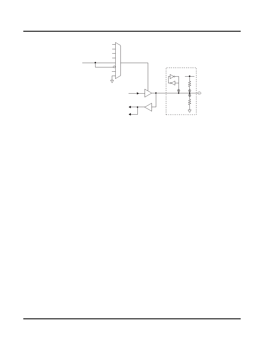
Figure 8. I/O Cell
Each output supports a variety of output standards dependent on the VCCO supplied to its I/O bank. Outputs can
also be congured for open drain operation. Each input can be programmed to support a variety of standards, inde-
pendent of the VCCO supplied to its I/O bank. The I/O standards supported are:
LVTTL
LVCMOS 1.8
LVCMOS 3.3
3.3V PCI Compatible
LVCMOS 2.5
All of the I/Os and dedicated inputs have the capability to provide a bus-keeper latch, Pull-up Resistor or Pull-down
Resistor. A fourth option is to provide none of these. The selection is done on a global basis. The default in both
hardware and software is such that when the device is erased or if the user does not specify, the input structure is
congured to be a Pull-up Resistor.
Each LA-ispMACH 4000V/Z automotive device I/O has an individually programmable output slew rate control bit.
Each output can be individually congured for fast slew or slow slew. The typical edge rate difference between fast
and slow slew setting is 20%. For high-speed designs with long, unterminated traces, the slow-slew rate will intro-
duce fewer reections, less noise and keep ground bounce to a minimum. For designs with short traces or well ter-
minated lines, the fast slew rate can be used to achieve the highest speed.
Global OE Generation
Most LA-ispMACH 4000V/Z automotive family devices have a 4-bit wide Global OE Bus, except the LA-ispMACH
4032V and LA-ispMACH4032Z devices that have a 2-bit wide Global OE Bus. This bus is derived from a 4-bit inter-
nal global OE PT bus and two dual purpose I/O or GOE pins. Each signal that drives the bus can optionally be
inverted.
Each GLB has a block-level OE PT that connects to all bits of the Global OE PT bus with four fuses. Hence, for a
128-macrocell device (with 16 blocks), each line of the bus is driven from 8 OE product terms. Figures 9 and 10
show a graphical representation of the global OE generation.
GOE 0
From ORP
*Global fuses
From ORP
To Macrocell
To GRP
GOE 1
GOE 2
GOE 3
VCC
VCCO
**
*
相關(guān)PDF資料 |
PDF描述 |
|---|---|
| EEM18DRST | CONN EDGECARD 36POS DIP .156 SLD |
| ISPLSI 2032A-80LJN44I | IC PLD ISP 32I/O 15NS 44PLCC |
| RCC70DRSN-S273 | CONN EDGECARD 140PS DIP .100 SLD |
| VI-BWH-CY-F4 | CONVERTER MOD DC/DC 52V 50W |
| ISPLSI 2032A-135LTN44 | IC PLD ISP 32I/O 7.5NS 44TQFP |
相關(guān)代理商/技術(shù)參數(shù) |
參數(shù)描述 |
|---|---|
| LA4064ZV-75TN100E | 制造商:LATTICE 制造商全稱:Lattice Semiconductor 功能描述:3.3V/1.8V In-System Programmable SuperFAST High Density PLDs |
| LA4064ZV-75TN128E | 制造商:LATTICE 制造商全稱:Lattice Semiconductor 功能描述:3.3V/1.8V In-System Programmable SuperFAST High Density PLDs |
| LA4064ZV-75TN144E | 制造商:LATTICE 制造商全稱:Lattice Semiconductor 功能描述:3.3V/1.8V In-System Programmable SuperFAST High Density PLDs |
| LA4064ZV-75TN44E | 制造商:LATTICE 制造商全稱:Lattice Semiconductor 功能描述:3.3V/1.8V In-System Programmable SuperFAST High Density PLDs |
| LA4064ZV-75TN48E | 制造商:LATTICE 制造商全稱:Lattice Semiconductor 功能描述:3.3V/1.8V In-System Programmable SuperFAST High Density PLDs |
發(fā)布緊急采購(gòu),3分鐘左右您將得到回復(fù)。