- 您現在的位置:買賣IC網 > PDF目錄369714 > L6917BDTR (意法半導體) 5 BIT PROGRAMMABLE DUAL-PHASE CONTROLLER PDF資料下載
參數資料
| 型號: | L6917BDTR |
| 廠商: | 意法半導體 |
| 英文描述: | 5 BIT PROGRAMMABLE DUAL-PHASE CONTROLLER |
| 中文描述: | 5位可編程雙相控制器 |
| 文件頁數: | 17/27頁 |
| 文件大小: | 411K |
| 代理商: | L6917BDTR |
第1頁第2頁第3頁第4頁第5頁第6頁第7頁第8頁第9頁第10頁第11頁第12頁第13頁第14頁第15頁第16頁當前第17頁第18頁第19頁第20頁第21頁第22頁第23頁第24頁第25頁第26頁第27頁
17/27
L6917
voltage drop due to the output capacitor discharge is given by the following equation:
Where D
MAX
is the maximum duty cycle value. The lower is the ESR, the lower is the output drop during load
transient and the lower is the output voltage static ripple.
Inductor design
The inductance value is defined by a compromise between the transient response time, the efficiency, the cost
and the size. The inductor has to be calculated to sustain the output and the input voltage variation to maintain
the ripple current
IL between 20% and 30% of the maximum output current. The inductance value can be cal-
culated with this relationship:
V
V
–
fs
Where f
S
is the switching frequency, V
IN
is the input voltage and V
OUT
is the output voltage.
Increasing the value of the inductance reduces the ripple current but, at the same time, reduces the converter
response time to a load transient. The response time is the time required by the inductor to change its current
from initial to final value. Since the inductor has not finished its charging time, the output current is supplied by
the output capacitors. Minimizing the response time can minimize the output capacitance required.
The response time to a load transient is different for the application or the removal of the load: if during the ap-
plication of the loadthe inductor is charged by a voltage equal to the difference between the input and the output
voltage, during the removal it is discharged only by the output voltage. The following expressions give approx-
imate response time for DI load transient in case of enough fast compensation network response:
The worst condition depends on the input voltage available and the output voltage selected. Anyway the worst
case is the response time after removal of the load with the minimum output voltage programmed and the max-
imum input voltage available.
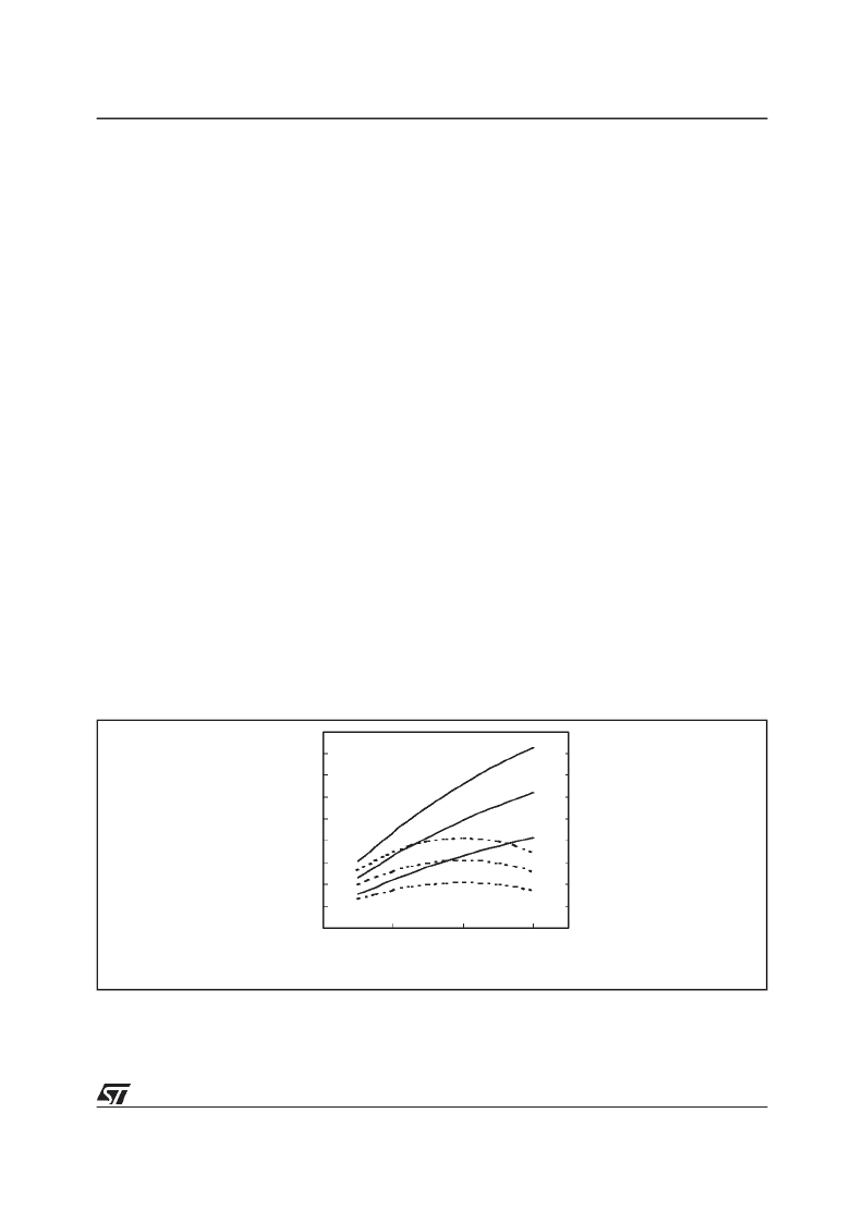
Figure 10. Inductor ripple current vs V
out
V
OUT
I
2
L
2 C
OUT
V
INMIN
D
MAX
V
OUT
–
)
--------------------------------------------------------------------------------------------
=
L
I
L
------------------------------
V
V
IN
---------------
=
t
application
V
OUT
V
IN
–
------------------------------
=
t
removal
V
OUT
I
---------------
=
0
1
2
3
4
5
6
7
8
9
0.5
1.5
2.5
3.5
Output Voltage [V]
I
L=3
μ
H,
Vin=12V
L=2
μ
H,
Vin=12V
L=1.5
μ
H, Vin=12V
L=2
μ
H,
Vin=5V
L=1.5
μ
H,
Vin=5V
L=3
μ
H, Vin=5V
相關PDF資料 |
PDF描述 |
|---|---|
| L6OV12 | Analog IC |
| L6OV15 | Analog IC |
| L6OV24 | Analog IC |
| L6OV5 | Analog IC |
| L6OV | Analog IC |
相關代理商/技術參數 |
參數描述 |
|---|---|
| L6917D | 制造商:未知廠家 制造商全稱:未知廠家 功能描述:Analog IC |
| L6917DTR | 制造商:未知廠家 制造商全稱:未知廠家 功能描述:Analog IC |
| L6918 | 制造商:STMICROELECTRONICS 制造商全稱:STMicroelectronics 功能描述:5 BIT PROGRAMMABLE MULTIPHASE CONTROLLER |
| L6918A | 制造商:STMICROELECTRONICS 制造商全稱:STMicroelectronics 功能描述:5 BIT PROGRAMMABLE MULTIPHASE CONTROLLER |
| L6918AD | 功能描述:DC/DC 開關控制器 Prog Multi-Phase Cnt RoHS:否 制造商:Texas Instruments 輸入電壓:6 V to 100 V 開關頻率: 輸出電壓:1.215 V to 80 V 輸出電流:3.5 A 輸出端數量:1 最大工作溫度:+ 125 C 安裝風格: 封裝 / 箱體:CPAK |
發(fā)布緊急采購,3分鐘左右您將得到回復。