- 您現(xiàn)在的位置:買賣IC網(wǎng) > PDF目錄384585 > L6452 (意法半導(dǎo)體) DUAL 13X16 MATRIX HEAD INK JET DRIVER PDF資料下載
參數(shù)資料
| 型號: | L6452 |
| 廠商: | 意法半導(dǎo)體 |
| 英文描述: | DUAL 13X16 MATRIX HEAD INK JET DRIVER |
| 中文描述: | 雙13X16矩陣驅(qū)動噴墨頭 |
| 文件頁數(shù): | 3/16頁 |
| 文件大小: | 115K |
| 代理商: | L6452 |
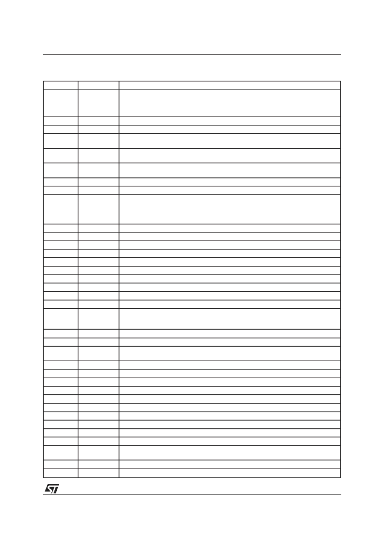
Pin #
30
Name
NCEn
Function
A high level enables the internal current sources and disables all DMOS outputs. To
be active, the internal current sources must have their corrsponding bit set inthe 16 bit
latchand Long Pulse must be set to low level. A low level enables the internalHSA/B
short circuit detection
A rising edge latches the 16 bit stored in the shift register in the 16 bit latch
Serial data input of the shift register
The data bit presented to the Serial Data Input pin is stored into the register on the
rising edge of this pin
A low level activates all outputshaving their coresponding bit in the 16bit latch set
(this pin has an internal pull-up resistor)
A low level activates all outputshaving their coresponding bit in the 16bit latch reset
(this pin has an internal pull-up resistor)
A low level disables all functions andclears all registers
A high level enables the A/D to start the new conversion
A/D clock signal; the ADDATA signal are valid onthe falling edge of this pin
If Nozzle Check Enable ishigh this output provides a high level when the open load is
detected on the output. If Nozzle Check Enable is low this output provides a high level
when a short circuitis detected on HSA/B output
Analogoutput signal (CH0 buffered)
A/D serial data output
Analogground connection
Ground of internal ADC
Power supply
Reference voltage generator
A/D input signals
Head selector address output channel B
Head Select Power Supply
Head selector address output channel A
A high level enables the counter and the internal decoder will activate of the HSx
outputsaccording to the counter’s outputs. SignalS0 becomesClock Counter and S1
becomes ResetCounter
A low level enables channel A and a high level enables channel B
Decoder input signals when Enable Counter is low
A high level enables the internal counter to upcounting. A low level enables down
counting
A low level resets the internal counter
A low level enables the selected channel (this input has an internal pull up resistor)
A high level clocks the internalcounter
Ground of step up block
Boost voltage
Driving voltage of power DMOS stage
5V logic supply
An external resistor connected versus ground fixes the internal current source value
Current source outputs
RxA, RxB voltage after an optional external filter
A low level enables the current source generator according the _A/B and ON/_OFF
control register bit
Data on pin CRdata are stored into the register on the rising edge of this pin
Control register serial data input
31
32
33
Latch Data
SDI
SDC
34
Long Pulse
35
Short Pulse
36
37
38
39
_Reset
ConvStart
ADCK
NCOut
40
41
42
43
CH0_buf
ADDATA
AnalogGND
ADCGND
Va
Vref
CH5..CH1
HSB1..HSB13
Vr
HSA13..HSA1
EnlC
44, 90
45
46 to 50
52 to 64
65
66 to 78
80
81
82
83
ChSel
S3
UpC/ S2
84
85
86
87
88
89
91
93
ResC/S1
_EnCh
ClkC/S0
Step up GND
Step up boost
Vstep up
VDD
Rext
RxB, RxA
VxA, VxB
_ONenable
94, 95
96, 97
98
99
100
CRclock
CRdata
PIN FUNCTIONS
(continued)
L6452
3/16
相關(guān)PDF資料 |
PDF描述 |
|---|---|
| L6561D013TR | POWER FACTOR CORRECTOR |
| L6569 | HIGH VOLTAGE HALF BRIDGE DRIVER WITH OSCILLATOR |
| L6569A | HIGH VOLTAGE HALF BRIDGE DRIVER WITH OSCILLATOR |
| L6569AD | HIGH VOLTAGE HALF BRIDGE DRIVER WITH OSCILLATOR |
| L6569D | HIGH VOLTAGE HALF BRIDGE DRIVER WITH OSCILLATOR |
相關(guān)代理商/技術(shù)參數(shù) |
參數(shù)描述 |
|---|---|
| L6452_06 | 制造商:STMICROELECTRONICS 制造商全稱:STMicroelectronics 功能描述:Dual 13x16 Matrix Head Ink Jet Driver |
| L64524 | 制造商:LSI Corporation 功能描述: |
| L6452DIE8 | 制造商:STMicroelectronics 功能描述: |
| L64550AGM | 制造商:未知廠家 制造商全稱:未知廠家 功能描述:Multifunction Peripheral |
| L64550AGMB | 制造商:未知廠家 制造商全稱:未知廠家 功能描述:Multifunction Peripheral |
發(fā)布緊急采購,3分鐘左右您將得到回復(fù)。