- 您現(xiàn)在的位置:買賣IC網(wǎng) > PDF目錄384534 > ISPGAL22V10C-15LKI (LATTICE SEMICONDUCTOR CORP) In-System Programmable E2CMOS PLD PDF資料下載
參數(shù)資料
| 型號(hào): | ISPGAL22V10C-15LKI |
| 廠商: | LATTICE SEMICONDUCTOR CORP |
| 元件分類: | PLD |
| 英文描述: | In-System Programmable E2CMOS PLD |
| 中文描述: | EE PLD, 15 ns, PDSO28 |
| 封裝: | 10.07 X 5.20 MM, SSOP-28 |
| 文件頁(yè)數(shù): | 10/15頁(yè) |
| 文件大?。?/td> | 247K |
| 代理商: | ISPGAL22V10C-15LKI |
第1頁(yè)第2頁(yè)第3頁(yè)第4頁(yè)第5頁(yè)第6頁(yè)第7頁(yè)第8頁(yè)第9頁(yè)當(dāng)前第10頁(yè)第11頁(yè)第12頁(yè)第13頁(yè)第14頁(yè)第15頁(yè)
Specifications
ispGAL22V10
10
ELECTRONIC SIGNATURE
An electronic signature (ES) is provided in every ispGAL22V10
device. It contains 64 bits of reprogrammable memory that can
contain user-defined data. Some uses include user ID codes,
revision numbers, or inventory control. The signature data is
always available to the user independent of the state of the
security cell.
The electronic signature is an additional feature not present in
other manufacturers' 22V10 devices. To use the extra feature of
the user-programmable electronic signature it is necessary to
choose a Lattice Semiconductor 22V10 device type when
compiling a set of logic equations. In addition, many device
programmers have two separate selections for the device,
typically an ispGAL22V10 and a ispGAL22V10-UES (UES =
User Electronic Signature) or ispGAL22V10-ES. This allows
users to maintain compatibility with existing 22V10 designs,
while still having the option to use the GAL device's extra
feature.
The JEDEC map for the ispGAL22V10 contains the 64 extra
fuses for the electronic signature, for a total of 5892 fuses.
However, the ispGAL22V10 device can still be programmed
with a standard 22V10 JEDEC map (5828 fuses) with any
qualified device programmer.
SECURITY CELL
A security cell is provided in every ispGAL22V10 device to
prevent unauthorized copying of the array patterns. Once
programmed, this cell prevents further read access to the
functional bits in the device. This cell can only be erased by re-
programming the device, so the original configuration can never
be examined once this cell is programmed. The Electronic
Signature is always available to the user, regardless of the state
of this control cell.
LATCH-UP PROTECTION
ispGAL22V10 devices are designed with an on-board charge
pump to negatively bias the substrate. The negative bias is of
sufficient magnitude to prevent input undershoots from causing
the circuitry to latch. Additionally, outputs are designed with n-
channel pullups instead of the traditional p-channel pullups to
eliminate any possibility of SCR induced latching.
DEVICE PROGRAMMING
The ispGAL22V10 device uses a standard 22V10 JEDEC
fusemap file to describe the device programming information.
Any third party logic compiler can produce the JEDEC file for this
device.
IN-SYSTEM PROGRAMMABILITY
The ispGAL22V10 device features In-System Programmable
technology. By integrating all the high voltage programming
circuitry on-chip, programming can be accomplished by simply
shifting data into the device. Once the function is programmed,
the non-volatile E
2
CMOS cells will not lose the pattern even
when the power is turned off.
All necessary programming is done via four TTL level logic
interface signals. These four signals are fed into the on-chip
programming circuitry where a state machine controls the pro-
gramming. The interface signals are Serial Data In (SDI), Serial
Data Out (SDO), Serial Clock (SCLK) and Mode (MODE)
control. For details on the operation of the internal state machine
and programming of ispGAL22V10 devices please refer to the
ISP Architecture and Programming section in this Data Book.
OUTPUT REGISTER PRELOAD
When testing state machine designs, all possible states and
state transitions must be verified in the design, not just those
required in the normal machine operations. This is because
certain events may occur during system operation that throw the
logic into an illegal state (power-up, line voltage glitches, brown-
outs, etc.). To test a design for proper treatment of these
conditions, a way must be provided to break the feedback paths,
and force any desired (i.e., illegal) state into the registers. Then
the machine can be sequenced and the outputs tested for
correct next state conditions.
The ispGAL22V10 device includes circuitry that allows each
registered output to be synchronously set either high or low.
Thus, any present state condition can be forced for test se-
quencing. If necessary, approved GAL programmers capable of
executing test vectors perform output register preload automati-
cally.
INPUT BUFFERS
ispGAL22V10 devices are designed with TTL level compatible
input buffers. These buffers have a characteristically high
impedance, and present a much lighter load to the driving logic
than bipolar TTL devices.
All input and I/O pins (except SDI on the ispGAL22V10C) also
have built-in active pull-ups. As a result, floating inputs will float
to a TTL high (logic 1). The SDI pin on the ispGAL22V10C has
a built-in pull-down to keep the device out of the programming
state if the pin is not actively driven. However, Lattice Semicon-
ductor recommends that all unused inputs and tri-stated I/O pins
be connected to an adjacent active input, Vcc, or ground. Doing
so will tend to improve noise immunity and reduce Icc for the
device. (See equivalent input and I/O schematics on the follow-
ing page.)
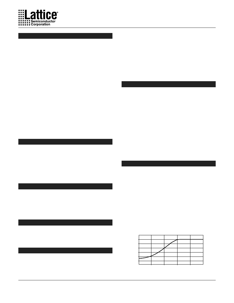
Typical Input Current
1.0
2.0
3.0
4.0 5.0
-60
0
-20
-40
0
Input Voltage (Volts)
I
μ
A
相關(guān)PDF資料 |
PDF描述 |
|---|---|
| ISPGAL22V10C-7LJ | In-System Programmable E2CMOS PLD |
| ISGAL22V10C-7LK | In-System Programmable E2CMOS PLD |
| ISPGDS14-7J | in-system programmable Generic Digital SwitchTM |
| ISPGDS14-7P | in-system programmable Generic Digital SwitchTM |
| ISPGDS18-7P | in-system programmable Generic Digital SwitchTM |
相關(guān)代理商/技術(shù)參數(shù) |
參數(shù)描述 |
|---|---|
| ISPGAL22V10C-7LJ | 功能描述:SPLD - 簡(jiǎn)單可編程邏輯器件 5V 22 I/O RoHS:否 制造商:Texas Instruments 邏輯系列:TICPAL22V10Z 大電池?cái)?shù)量:10 最大工作頻率:66 MHz 延遲時(shí)間:25 ns 工作電源電壓:4.75 V to 5.25 V 電源電流:100 uA 最大工作溫度:+ 75 C 最小工作溫度:0 C 安裝風(fēng)格:Through Hole 封裝 / 箱體:DIP-24 |
| ISPGAL22V10C-7LJN | 功能描述:SPLD - 簡(jiǎn)單可編程邏輯器件 PROGRAMMABLE LO VOLT E2CMOS PLD RoHS:否 制造商:Texas Instruments 邏輯系列:TICPAL22V10Z 大電池?cái)?shù)量:10 最大工作頻率:66 MHz 延遲時(shí)間:25 ns 工作電源電壓:4.75 V to 5.25 V 電源電流:100 uA 最大工作溫度:+ 75 C 最小工作溫度:0 C 安裝風(fēng)格:Through Hole 封裝 / 箱體:DIP-24 |
| ISPGAL22V10C-7LK | 功能描述:SPLD - 簡(jiǎn)單可編程邏輯器件 PROGRAMMABLE LO VOLT E2CMOS PLD RoHS:否 制造商:Texas Instruments 邏輯系列:TICPAL22V10Z 大電池?cái)?shù)量:10 最大工作頻率:66 MHz 延遲時(shí)間:25 ns 工作電源電壓:4.75 V to 5.25 V 電源電流:100 uA 最大工作溫度:+ 75 C 最小工作溫度:0 C 安裝風(fēng)格:Through Hole 封裝 / 箱體:DIP-24 |
| ISPGDS14-7J | 功能描述:CPLD - 復(fù)雜可編程邏輯器件 PROGRAMMABLE GEN DIGITAL SWITCH RoHS:否 制造商:Lattice 系列: 存儲(chǔ)類型:EEPROM 大電池?cái)?shù)量:128 最大工作頻率:333 MHz 延遲時(shí)間:2.7 ns 可編程輸入/輸出端數(shù)量:64 工作電源電壓:3.3 V 最大工作溫度:+ 90 C 最小工作溫度:0 C 封裝 / 箱體:TQFP-100 |
| ISPGDS14-7P | 制造商:Rochester Electronics LLC 功能描述:- Bulk |
發(fā)布緊急采購(gòu),3分鐘左右您將得到回復(fù)。