- 您現(xiàn)在的位置:買(mǎi)賣(mài)IC網(wǎng) > PDF目錄10588 > ISLA222P20IRZ (Intersil)IC ADC 12BIT SRL/SPI 72QFN PDF資料下載
參數(shù)資料
| 型號(hào): | ISLA222P20IRZ |
| 廠商: | Intersil |
| 文件頁(yè)數(shù): | 19/33頁(yè) |
| 文件大?。?/td> | 0K |
| 描述: | IC ADC 12BIT SRL/SPI 72QFN |
| 標(biāo)準(zhǔn)包裝: | 1 |
| 系列: | FemtoCharge™ |
| 位數(shù): | 12 |
| 采樣率(每秒): | 200M |
| 數(shù)據(jù)接口: | 串行,SPI? |
| 轉(zhuǎn)換器數(shù)目: | 2 |
| 功率耗散(最大): | 830mW |
| 電壓電源: | 模擬和數(shù)字 |
| 工作溫度: | -40°C ~ 85°C |
| 安裝類(lèi)型: | 表面貼裝 |
| 封裝/外殼: | 72-VFQFN 裸露焊盤(pán) |
| 供應(yīng)商設(shè)備封裝: | 72-QFN(10x10) |
| 包裝: | 托盤(pán) |
| 輸入數(shù)目和類(lèi)型: | * |
第1頁(yè)第2頁(yè)第3頁(yè)第4頁(yè)第5頁(yè)第6頁(yè)第7頁(yè)第8頁(yè)第9頁(yè)第10頁(yè)第11頁(yè)第12頁(yè)第13頁(yè)第14頁(yè)第15頁(yè)第16頁(yè)第17頁(yè)第18頁(yè)當(dāng)前第19頁(yè)第20頁(yè)第21頁(yè)第22頁(yè)第23頁(yè)第24頁(yè)第25頁(yè)第26頁(yè)第27頁(yè)第28頁(yè)第29頁(yè)第30頁(yè)第31頁(yè)第32頁(yè)第33頁(yè)
ISLA222P
26
FN7853.1
June 17, 2011
ADDRESS 0X74: OUTPUT_MODE_B
Bit 6 DLL Range
This bit sets the DLL operating range to fast (default) or slow.
Internal clock signals are generated by a delay-locked loop (DLL),
which has a finite operating range. Table 12 shows the allowable
sample rate ranges for the slow and fast settings.
ADDRESS 0XB6: CALIBRATION STATUS
The LSB at address 0xB6 can be read to determine calibration
status. The bit is ‘0’ during calibration and goes to a logic ‘1’
when calibration is complete. This register is unique in that it can
be read after POR at calibration, unlike the other registers on
chip, which can’t be read until calibration is complete.
DEVICE TEST
The ISLA222P can produce preset or user defined patterns on
the digital outputs to facilitate in-situ testing. A user can pick
from preset built-in patterns by writing to the output test mode
field [7:4] at 0xC0 or user defined patterns by writing to the user
test mode field [2:0] at 0xC0. The user defined patterns should
be loaded at address space 0xC1 through 0xD0, see the “SPI
Memory Map” on page 28 for more detail. The predefined
patterns are shown in Table 13. The test mode is enabled
asynchronously to the sample clock; therefore several sample
clock cycles may elapse before the data is present on the output
bus.
ADDRESS 0XC0: TEST_IO
Bits 7:4 Output Test Mode
These bits set the test mode according to Table 13. Other
values are reserved. User test patterns loaded at 0xC1 through
0xD0 are also available by writing ‘1000’ to [7:4] at 0xC0 and a
pattern depth value to [2:0] at 0xC0. See the “SPI Memory
Bits 2:0 User Test Mode
The three LSBs in this register determine the test pattern in
combination with registers 0xC1 through 0xD0. Refer to the
ADDRESS 0XC1: USER_PATT1_LSB
ADDRESS 0XC2: USER_PATT1_MSB
These registers define the lower and upper eight bits,
respectively, of the user-defined pattern 1.
ADDRESS 0XC3: USER_PATT2_LSB
ADDRESS 0XC4: USER_PATT2_MSB
These registers define the lower and upper eight bits,
respectively, of the user-defined pattern 2
ADDRESS 0XC5: USER_PATT3_LSB
ADDRESS 0XC6: USER_PATT3_MSB
These registers define the lower and upper eight bits,
respectively, of the user-defined pattern 3
ADDRESS 0XC7: USER_PATT4_LSB
ADDRESS 0XC8: USER_PATT4_MSB
These registers define the lower and upper eight bits,
respectively, of the user-defined pattern 4.
ADDRESS 0XC9: USER_PATT5_LSB
ADDRESS 0XCA: USER_PATT5_MSB
These registers define the lower and upper eight bits,
respectively, of the user-defined pattern 5.
ADDRESS 0XCB: USER_PATT6_LSB
ADDRESS 0XCC: USER_PATT6_MSB
These registers define the lower and upper eight bits,
respectively, of the user-defined pattern 6
ADDRESS 0XCD: USER_PATT7_LSB
ADDRESS 0XCE: USER_PATT7_MSB
These registers define the lower and upper eight bits,
respectively, of the user-defined pattern 7.
ADDRESS 0XCF: USER_PATT8_LSB
ADDRESS 0XD0: USER_PATT8_MSB
These registers define the lower and upper eight bits,
respectively, of the user-defined pattern 8.
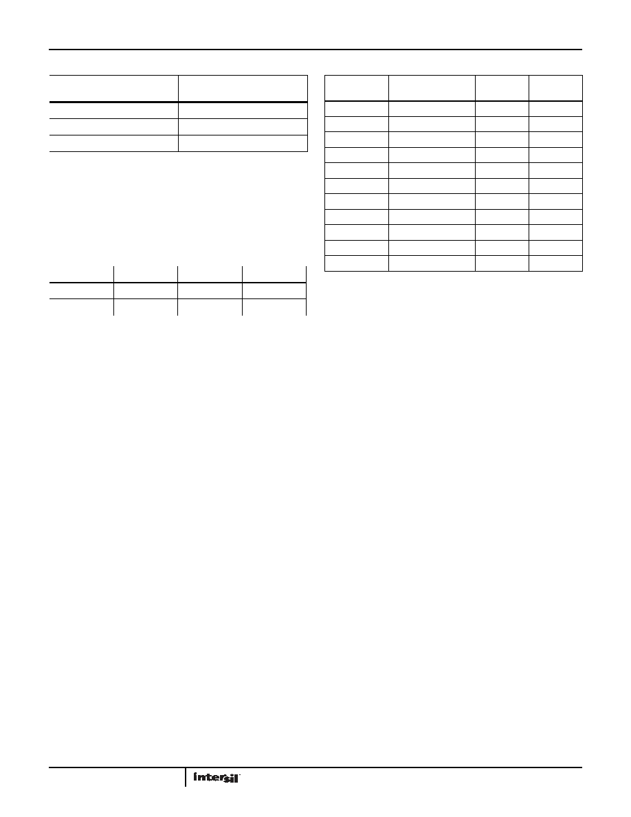
TABLE 11. OUTPUT FORMAT CONTROL
VALUE
0x73[2:0]
OUTPUT FORMAT
000
Two’s Complement (Default)
010
Gray Code
100
Offset Binary
TABLE 12. DLL RANGES
DLL RANGE
MIN
MAX
UNIT
Slow
40
100
MSPS
Fast
80
250
MSPS
TABLE 13. OUTPUT TEST MODES
VALUE
0xC0[7:4]
OUTPUT TEST MODE
WORD 1
WORD 2
0000
Off
0001
Midscale
0x8000
N/A
0010
Positive Full-Scale
0xFFFF
N/A
0011
Negative Full-Scale
0x0000
N/A
0100
Reserved
N/A
0101
Reserved
N/A
0110
Reserved
N/A
0111
Reserved
1000
User Pattern
user_patt1
user_patt2
1001
Reserved
N/A
1010
Ramp
N/A
相關(guān)PDF資料 |
PDF描述 |
|---|---|
| LMH0002TMAX/NOPB | IC CABLE DVR SERIAL DGTL 8-SOIC |
| KAD2710L-27Q68 | IC ADC 10BIT 275MSPS SGL 68-QFN |
| VE-27L-IW-F4 | CONVERTER MOD DC/DC 28V 100W |
| LMH0002SQX/NOPB | IC CABLE DVR SERIAL DGTL 16-LLP |
| LMH0002MAX/NOPB | IC CABLE DRIVER DGTL 8-SOIC |
相關(guān)代理商/技術(shù)參數(shù) |
參數(shù)描述 |
|---|---|
| ISLA222P25 | 制造商:INTERSIL 制造商全稱:Intersil Corporation 功能描述:Dual 14-Bit, 250MSPS/200MSPS/130MSPS ADC |
| ISLA222P25IRZ | 制造商:Intersil Corporation 功能描述:12-BIT 250MSPS DUAL ADC, 72-PIN QFN - Trays 制造商:Intersil Corporation 功能描述:IC ADC 12BIT SRL/SPI 72QFN 制造商:Intersil 功能描述:12-BIT 250MSPS DL AD C 72-PIN |
| ISLA222S | 制造商:INTERSIL 制造商全稱:Intersil Corporation 功能描述:Dual 12-Bit, 250/200/125 MSPS JESD204B High Speed Serial Output ADC |
| ISLA222S12 | 制造商:INTERSIL 制造商全稱:Intersil Corporation 功能描述:Dual 14-Bit, 250/200/125 MSPS JESD204B High Speed Serial Output ADC |
| ISLA222S12IR1Z | 制造商:Intersil Corporation 功能描述:DUAL 12-BIT, 125MSPS ADC W/HIGH SPEED SERIAL JESD204B OUTPUT - Trays 制造商:Intersil Corporation 功能描述:IC ADC 12BIT SPI/SRL 125M 48LQFN |
發(fā)布緊急采購(gòu),3分鐘左右您將得到回復(fù)。