- 您現(xiàn)在的位置:買賣IC網(wǎng) > PDF目錄3390 > ISL28108FBZ-T7 (Intersil)IC OPAMP GP RR 1.2MHZ 8SOIC PDF資料下載
參數(shù)資料
| 型號(hào): | ISL28108FBZ-T7 |
| 廠商: | Intersil |
| 文件頁數(shù): | 14/34頁 |
| 文件大小: | 0K |
| 描述: | IC OPAMP GP RR 1.2MHZ 8SOIC |
| 標(biāo)準(zhǔn)包裝: | 1,000 |
| 放大器類型: | 通用 |
| 電路數(shù): | 1 |
| 輸出類型: | 滿擺幅 |
| 轉(zhuǎn)換速率: | 0.45 V/µs |
| 增益帶寬積: | 1.2MHz |
| 電流 - 輸入偏壓: | 13nA |
| 電壓 - 輸入偏移: | 25µV |
| 電流 - 電源: | 185µA |
| 電流 - 輸出 / 通道: | 30mA |
| 電壓 - 電源,單路/雙路(±): | 3 V ~ 40 V,±1.5 V ~ 20 V |
| 工作溫度: | -40°C ~ 125°C |
| 安裝類型: | 表面貼裝 |
| 封裝/外殼: | 8-SOIC(0.154",3.90mm 寬) |
| 供應(yīng)商設(shè)備封裝: | 8-SOIC |
| 包裝: | 帶卷 (TR) |
第1頁第2頁第3頁第4頁第5頁第6頁第7頁第8頁第9頁第10頁第11頁第12頁第13頁當(dāng)前第14頁第15頁第16頁第17頁第18頁第19頁第20頁第21頁第22頁第23頁第24頁第25頁第26頁第27頁第28頁第29頁第30頁第31頁第32頁第33頁第34頁
ISL28108, ISL28208, ISL28408
FN6935.5
March 4, 2014
Applications Information
Functional Description
The ISL28108, ISL28208, and ISL28408 are single, dual and
quad, 1.2MHz, single supply rail-to-rail output amplifiers with a
common mode input voltage range extending to a range of 0.5V
below the V- rail. Their input stages are optimized for precision
sensing of ground referenced signals in low voltage, single supply
applications. The input stage has the capability of handling large
input differential voltages without phase inversion making them
suitable for high voltage comparator applications. Their bipolar
design features high open loop gain and excellent DC input and
output temperature stability. These op amps feature low quiescent
current of 165A, and a maximum temperature drift ranging from
1.1V/°C for the ISL28208 and ISL28408 in the SOIC package to
1.4V/°C for the ISL28208 in the TDFN package and the ISL28408
fabricated in a new precision 40V complementary bipolar DI process
and immune from latch-up.
Operating Voltage Range
The devices are designed to operate over the 3V (±1.5V) to
40V (±20V) range and are fully characterized at ±5V and ±15V. Both
DC and AC performance remain virtually unchanged over the ±5V
to ±15V operating voltage range. Parameter variation with
operating voltage is shown in the “Typical Performance Curves”
beginning on page 10.
Input Stage Performance
The PNP input stage has a common mode input range extending
amplifier performance is guaranteed down to ground (V-) over the
-40°C to +125°C temperature range. For common mode voltages
down to -0.5V the amplifiers are fully functional, but performance
degrades slightly over the full temperature range. This feature
provides excellent CMRR, AC performance and DC accuracy when
amplifying low level ground referenced signals.
The input stage has a maximum input differential voltage equal
to a diode drop greater than the supply voltage (max 42V) and
does not contain the back-to-back input protection diodes found
on many similar amplifiers. This feature enables the device to
function as a precision comparator by maintaining very high
input impedance for high voltage differential input comparator
voltages. The high differential input impedance also enables the
device to operate reliably in large signal pulse applications
without the need for anti-parallel clamp diodes required on
MOSFET and most bipolar input stage op amps. Thus, input
signal distortion caused by nonlinear clamps under high slew
rate conditions are avoided.
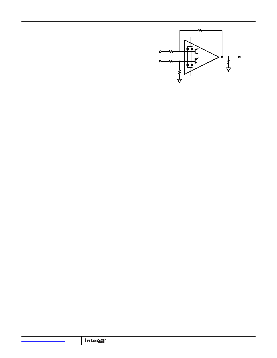
In applications where one or both amplifier input terminals are at
risk of exposure to voltages beyond the supply rails, current
limiting resistors may be needed at each input terminal
supply ESD diodes to 20mA.
Output Drive Capability
The bipolar rail-to-rail output stage features low saturation levels
that enable an output voltage swing to less than 10mV when the
total output load (including feedback resistance) is held below
achieved by using feedback resistor values >300k. The low input
bias and offset currents (-43nA and ±3nA +25°C max
respectively) minimize DC offset errors at these high resistance
values. For example, a balanced 4 resistor gain circuit (Figure 65)
with 1M feedback resistors (RF, RG) generates a worst case
input offset error of only ±3mV. Furthermore, the low noise
current reduces the added noise associated with high feedback
resistance.
The output stage is internally current limited. Output current limit
can withstand a short circuit to either rail as long as the power
dissipation limits are not exceeded. This applies to only one
amplifier at a time for the dual op amp. Continuous operation
under these conditions may degrade long-term reliability.
The amplifiers perform well driving capacitive loads
configuration provides the highest bandwidth, but is also the
most sensitive to ringing produced by load capacitance found in
BNC cables. Unity gain overshoot is limited to 30% at
capacitance values to 0.33nF. At gains of 10 and higher, the
device is capable of driving more than 10nF without significant
overshoot.
Output Phase Reversal
Output phase reversal is a change of polarity in the amplifier
transfer function when the input voltage exceeds the supply
voltage. These devices are immune to output phase reversal, out
FIGURE 65. INPUT ESD DIODE CURRENT LIMITING
-
+
RIN-
RL
VIN-
V+
V-
RIN+
VIN+
RF
RG
相關(guān)PDF資料 |
PDF描述 |
|---|---|
| TLC2272CPSG4 | IC OPAMP GP R-R 2.25MHZ 8SOIC |
| 961238-6700-AR-PT | CONN HEADER STR DL 38PS GOLD SMD |
| 53610-S20-4 | EJC LTC.100"SHD HD.0100"VER 15GD |
| 108457096002049 | CONN HEADER MALE 96POS R/A |
| 1.5KE68ARL4G | TVS 1500W 68V UNIDIRECT AXIAL |
相關(guān)代理商/技術(shù)參數(shù) |
參數(shù)描述 |
|---|---|
| ISL28108FBZ-T7A | 功能描述:運(yùn)算放大器 - 運(yùn)放 ISL28108FBZ 40V LW PWR RAIL-RAIL OUT RoHS:否 制造商:STMicroelectronics 通道數(shù)量:4 共模抑制比(最小值):63 dB 輸入補(bǔ)償電壓:1 mV 輸入偏流(最大值):10 pA 工作電源電壓:2.7 V to 5.5 V 安裝風(fēng)格:SMD/SMT 封裝 / 箱體:QFN-16 轉(zhuǎn)換速度:0.89 V/us 關(guān)閉:No 輸出電流:55 mA 最大工作溫度:+ 125 C 封裝:Reel |
| ISL28108FRTZ | 功能描述:放大器 IC 開發(fā)工具 ISL28108FRTZ 40V LW PWR R-R OUT SNGL SUP RoHS:否 制造商:International Rectifier 產(chǎn)品:Demonstration Boards 類型:Power Amplifiers 工具用于評估:IR4302 工作電源電壓:13 V to 23 V |
| ISL28108FRTZ-T13 | 功能描述:放大器 IC 開發(fā)工具 ISL28108FRTZ 40V LW PWR R-R OUT SNGL SUP RoHS:否 制造商:International Rectifier 產(chǎn)品:Demonstration Boards 類型:Power Amplifiers 工具用于評估:IR4302 工作電源電壓:13 V to 23 V |
| ISL28108FRTZ-T7 | 功能描述:放大器 IC 開發(fā)工具 ISL28108FRTZ 40V LW PWR R-R OUT SNGL SUP RoHS:否 制造商:International Rectifier 產(chǎn)品:Demonstration Boards 類型:Power Amplifiers 工具用于評估:IR4302 工作電源電壓:13 V to 23 V |
| ISL28108FRTZ-T7A | 功能描述:運(yùn)算放大器 - 運(yùn)放 ISL28108FRTZ 40V LW RAIL OUT SNG SUPP RoHS:否 制造商:STMicroelectronics 通道數(shù)量:4 共模抑制比(最小值):63 dB 輸入補(bǔ)償電壓:1 mV 輸入偏流(最大值):10 pA 工作電源電壓:2.7 V to 5.5 V 安裝風(fēng)格:SMD/SMT 封裝 / 箱體:QFN-16 轉(zhuǎn)換速度:0.89 V/us 關(guān)閉:No 輸出電流:55 mA 最大工作溫度:+ 125 C 封裝:Reel |
發(fā)布緊急采購,3分鐘左右您將得到回復(fù)。