- 您現(xiàn)在的位置:買賣IC網(wǎng) > PDF目錄385448 > IRS21303STRPbF (International Rectifier) 3-PHASE BRIDGE DRIVER PDF資料下載
參數(shù)資料
| 型號: | IRS21303STRPbF |
| 廠商: | International Rectifier |
| 英文描述: | 3-PHASE BRIDGE DRIVER |
| 中文描述: | 3相橋式驅(qū)動器 |
| 文件頁數(shù): | 11/22頁 |
| 文件大小: | 530K |
| 代理商: | IRS21303STRPBF |
www.irf.com
11
IRS2130/IRS21303/IRS2132 (J&S)PbF
1 PCB Layout Tips
1.1 Distance from H to L Voltage
The IRS213(0,03,2)J package lacks some pins (see page 8) in order to maximizing the distance between the high
voltage and low voltage pins. It’s strongly recommended to place the components tied to the floating voltage in the
respective high voltage portions of the device (V
B1,2,3
, V
S1,2,3
) side.
1.2 Ground Plane
To minimize noise coupling the ground plane must not be placed under or near the high voltage floating side.
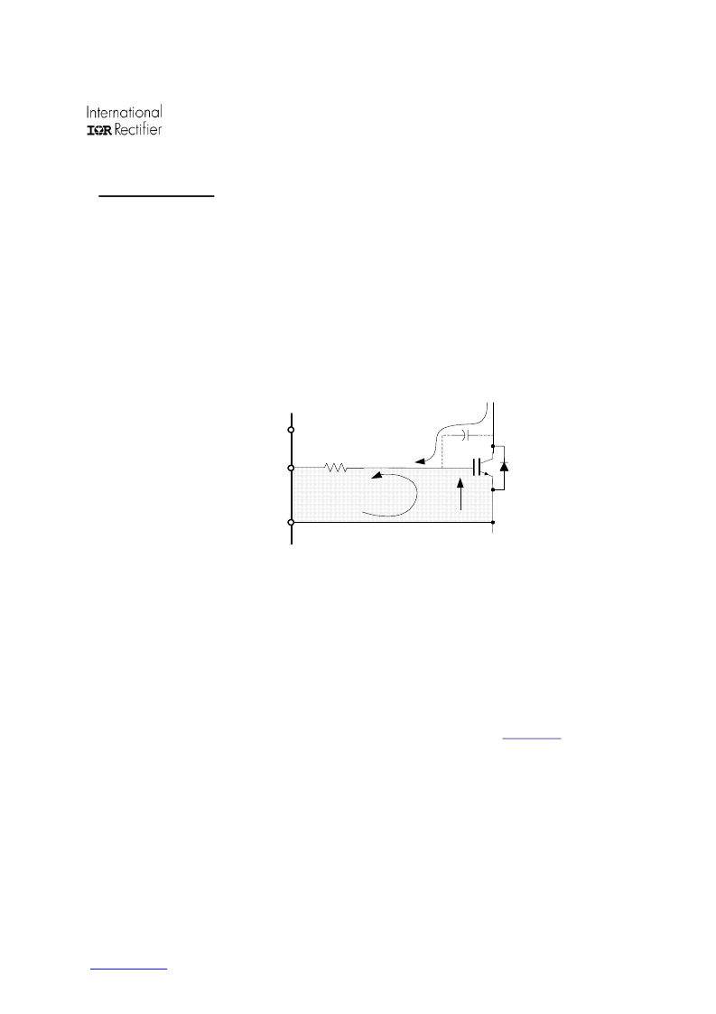
1.3 Gate Drive Loops
Current loops behave like an antenna able to receive and transmit EM noise (see Fig. 7). In order to reduce EM
coupling and improve the power switch turn on/off performances, gate drive loops must be reduced as much as
possible. Moreover, current can be injected inside the gate drive loop via the IGBT collector-to-gate parasitic
capacitance. The parasitic auto-inductance of the gate loop contributes to develop a voltage across the gate-emitter
increasing the possibility of self turn-on effect.
Fig. 7. Antenna Loops
1.4 Supply Capacitors
Supply capacitors must be placed as close as possible to the device pins (V
CC
and V
SS
for the ground tied supply, V
B
and V
S
for the floating supply) in order to minimize parasitic inductance/resistance.
1.5 Routing and Placement
Power stage PCB parasitic may generate dangerous voltage transients for the gate driver and the control logic. In
particular it’s recommended to limit phase voltage negative transients.
In order to avoid such undervoltage it is highly recommended to minimize high side emitter to low side collector
distance and low side emitter to negative bus rail stray inductance. See DT04-4 at
www.irf.com
for more detailed
information.
gate
resistance
V
SX
( Vs0 )
V
BX
(V
CC
)
HO
X
(LO
X
)
V
GE
Gate Drive
Loop
C
GC
I
GC
PRELIMINARY
相關(guān)PDF資料 |
PDF描述 |
|---|---|
| IRS2130PbF | 3-PHASE BRIDGE DRIVER |
| IRS2130SPbF | 3-PHASE BRIDGE DRIVER |
| IRS2130STRPbF | 3-PHASE BRIDGE DRIVER |
| IRS2132 | 3-PHASE BRIDGE DRIVER |
| IRS2132JPbF | 3-PHASE BRIDGE DRIVER |
相關(guān)代理商/技術(shù)參數(shù) |
參數(shù)描述 |
|---|---|
| IRS2130D | 制造商:IRF 制造商全稱:International Rectifier 功能描述:3-PHASE BRIDGE DRIVER |
| IRS2130DPBF | 制造商:IRF 制造商全稱:International Rectifier 功能描述:3-PHASE BRIDGE DRIVER |
| IRS2130DSPBF | 制造商:IRF 制造商全稱:International Rectifier 功能描述:3-PHASE BRIDGE DRIVER |
| IRS2130JTRPBF | 制造商:IRF 制造商全稱:International Rectifier 功能描述:3-PHASE BRIDGE DRIVER |
| IRS2130PBF | 制造商:IRF 制造商全稱:International Rectifier 功能描述:3-PHASE BRIDGE DRIVER |
發(fā)布緊急采購,3分鐘左右您將得到回復(fù)。