- 您現(xiàn)在的位置:買(mǎi)賣(mài)IC網(wǎng) > PDF目錄65584 > IDT74FCT16652CTPAG (INTEGRATED DEVICE TECHNOLOGY INC) FCT SERIES, DUAL 8-BIT REGISTERED TRANSCEIVER, TRUE OUTPUT, PDSO56 PDF資料下載
參數(shù)資料
| 型號(hào): | IDT74FCT16652CTPAG |
| 廠商: | INTEGRATED DEVICE TECHNOLOGY INC |
| 元件分類(lèi): | 總線收發(fā)器 |
| 英文描述: | FCT SERIES, DUAL 8-BIT REGISTERED TRANSCEIVER, TRUE OUTPUT, PDSO56 |
| 封裝: | TSSOP-56 |
| 文件頁(yè)數(shù): | 1/9頁(yè) |
| 文件大?。?/td> | 102K |
| 代理商: | IDT74FCT16652CTPAG |
1
IDT74FCT16652AT/CT
FASTCMOS16-BITBUSTRANSCEIVER/REGISTER
INDUSTRIALTEMPERATURERANGE
JUNE 2002
IDT74FCT16652AT/CT
INDUSTRIAL TEMPERATURE RANGE
FAST CMOS 16-BIT BUS
TRANSCEIVER/REGISTER
DESCRIPTION:
The FCT16652T 16-bit registered transceivers are built using advanced
dual metal CMOS technology. These high-speed, low-power devices are
organized as two independent 8-bit bus transceivers with 3-state D-type
registers.Forexample,thexOEABandxOEBAsignalscontrolthetransceiver
functions.
The xSAB and xSBA control pins are provided to select either real time or
storeddatatransfer. Thecircuitryusedforselectcontrolwilleliminatethetypical
decodingglitchthatoccursinamultiplexerduringthetransitionbetweenstored
andrealtimedata.Alowinputlevelselectsreal-timedataandahighlevelselects
storeddata.
DataontheAorBdatabus,orboth,canbestoredintheinternalD-flip-flops
bylow-to-hightransitionsattheappropriateclockpins(xCLKABorxCLKBA),
regardless of the select or enable control pins. Flow-through organization of
signalpinssimplifieslayout.Allinputsaredesignedwithhysteresisforimproved
noisemargin.
TheFCT16652Tisideallysuitedfordrivinghighcapacitanceloadsandlow-
impedancebackplanes.Theoutputbuffersaredesignedwithpoweroffdisable
capability to allow "live insertion" of boards when used as backplane drivers.
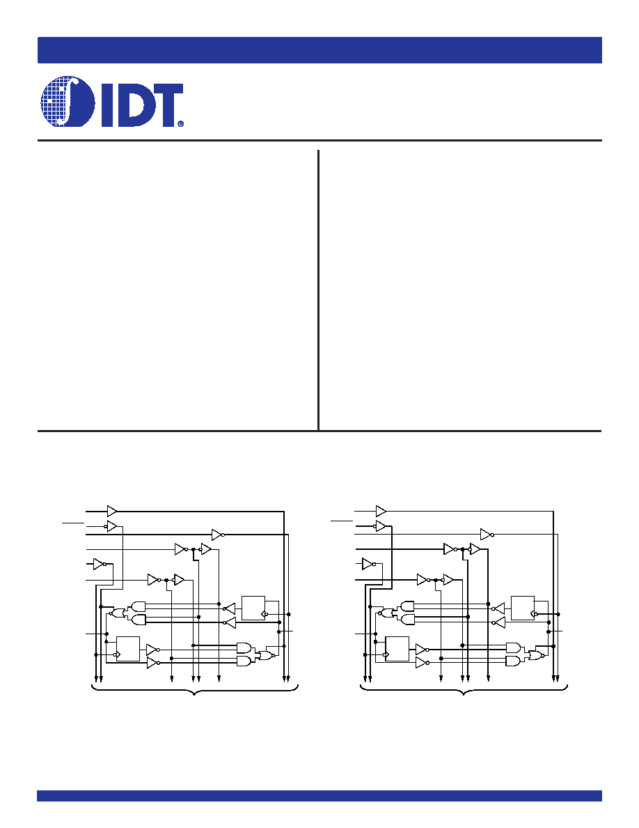
1
A1
1
O EBA
1
CLKBA
1
SBA
1
CLKAB
1
SAB
1
OE AB
1
B1
B R EG
A R EG
D
C
D
TO S E VE N O THE R CHA NNELS
2
B 1
2
CLK AB
2
O EBA
2
CLK BA
2
SBA
2
A1
2
O EAB
2
SAB
TO SEVEN O THE R CHANNE LS
B R EG
A R EG
D
C
D
FEATURES:
0.5 MICRON CMOS Technology
High-speed, low-power CMOS replacement for ABT functions
Typical tSK(o) (Output Skew) < 250ps
Low input and output leakage
≤≤≤≤≤1A (max.)
VCC = 5V ±10%
High drive outputs (–32mA IOH, 64mA IOL)
Power off disable outputs permit “l(fā)ive insertion”
Typical VOLP (Output Ground Bounce) < 1.0V at VCC = 5V,
TA = 25°C
Available in SSOP and TSSOP packages
FUNCTIONAL BLOCK DIAGRAM
The IDT logo is a registered trademark of Integrated Device Technology, Inc.
2002 Integrated Device Technology, Inc.
DSC-5450/2
相關(guān)PDF資料 |
PDF描述 |
|---|---|
| IDT74FCT16652ETPVT/R | FCT SERIES, DUAL 8-BIT REGISTERED TRANSCEIVER, TRUE OUTPUT, PDSO56 |
| IDT74FCT16823BTPV8 | FCT SERIES, DUAL 9-BIT DRIVER, TRUE OUTPUT, PDSO56 |
| IDT74FCT16823ETPF8 | FCT SERIES, DUAL 9-BIT DRIVER, TRUE OUTPUT, PDSO56 |
| IDT74FCT16827ATPA8 | FCT SERIES, DUAL 10-BIT DRIVER, TRUE OUTPUT, PDSO56 |
| IDT74FCT16827CTPV8 | FCT SERIES, DUAL 10-BIT DRIVER, TRUE OUTPUT, PDSO56 |
相關(guān)代理商/技術(shù)參數(shù) |
參數(shù)描述 |
|---|---|
| IDT74FCT16652TPA | 制造商:Integrated Device Technology Inc 功能描述: |
| IDT74FCT16652TPV | 制造商:Integrated Device Technology Inc 功能描述: |
| IDT74FCT16823ATPV | 制造商:INT_DEV_TECH 功能描述: |
| IDT74FCT16823CTPV | 制造商:Integrated Device Technology Inc 功能描述: |
| IDT74FCT16823ETPA | 制造商:Integrated Device Technology Inc 功能描述: |
發(fā)布緊急采購(gòu),3分鐘左右您將得到回復(fù)。