- 您現(xiàn)在的位置:買賣IC網(wǎng) > PDF目錄9968 > IDT72V3654L15PF (IDT, Integrated Device Technology Inc)IC BI FIFO 4096X36 15NS 128QFP PDF資料下載
參數(shù)資料
| 型號: | IDT72V3654L15PF |
| 廠商: | IDT, Integrated Device Technology Inc |
| 文件頁數(shù): | 26/37頁 |
| 文件大小: | 0K |
| 描述: | IC BI FIFO 4096X36 15NS 128QFP |
| 標準包裝: | 36 |
| 系列: | 72V |
| 功能: | 異步 |
| 存儲容量: | 147K(4K x 36) |
| 數(shù)據(jù)速率: | 67MHz |
| 訪問時間: | 15ns |
| 電源電壓: | 3.15 V ~ 3.45 V |
| 工作溫度: | 0°C ~ 70°C |
| 安裝類型: | 表面貼裝 |
| 封裝/外殼: | 128-LQFP |
| 供應(yīng)商設(shè)備封裝: | 128-TQFP(14x20) |
| 包裝: | 托盤 |
| 其它名稱: | 72V3654L15PF |
第1頁第2頁第3頁第4頁第5頁第6頁第7頁第8頁第9頁第10頁第11頁第12頁第13頁第14頁第15頁第16頁第17頁第18頁第19頁第20頁第21頁第22頁第23頁第24頁第25頁當前第26頁第27頁第28頁第29頁第30頁第31頁第32頁第33頁第34頁第35頁第36頁第37頁
32
COMMERCIALTEMPERATURERANGE
IDT72V3654/72V3664/72V3674 3.3V CMOS SyncBiFIFOTM WITH BUS-MATCHING
2,048 x 36 x 2, 4,096 x 36 x 2 and 8,192 x 36 x 2
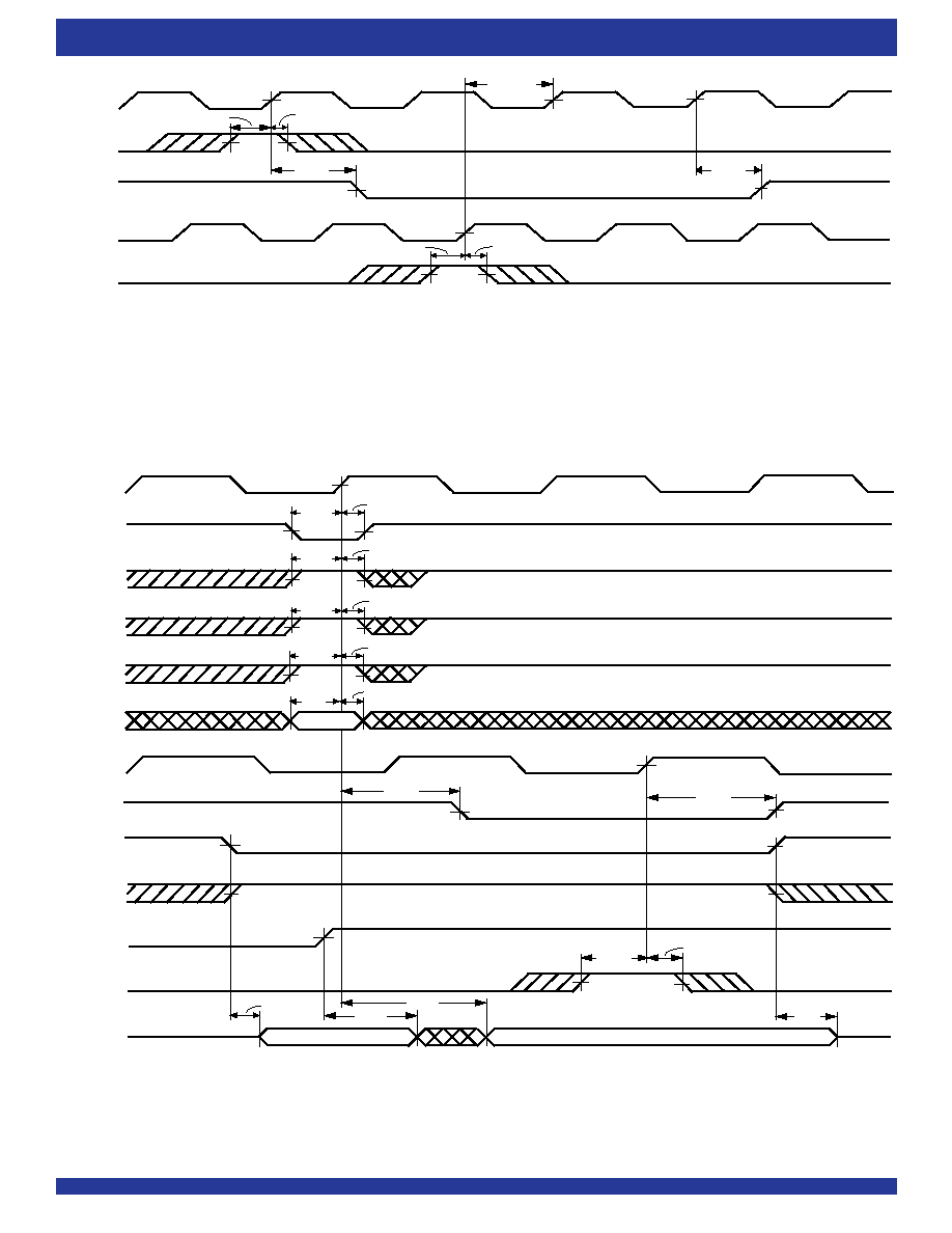
Figure 26. Timing for
AFB
AFB when FIFO2 is Almost-Full (IDT Standard and FWFT Modes)
Figure 27. Timing for Mail1 Register and
MBF1
MBF1 Flag (IDT Standard and FWFT Modes)
NOTE:
1. If Port B is configured for word size, data can be written to the Mail1 register using A0-A17 (A18-A35 are don't care inputs). In this first case B0-B17 will have valid data (B18-B35
will be indeterminate). If Port B is configured for byte size, data can be written to the Mail1 Register using A0-A8 (A9-A35 are don't care inputs). In this second case, B0-B8 will
have valid data (B9-B35 will be indeterminate).
NOTES:
1. tSKEW2 is the minimum time between a rising CLKB edge and a rising CLKA edge for
AFB to transition HIGH in the next CLKB cycle. If the time between the rising CLKB edge and rising
CLKA edge is less than tSKEW2, then
AFB may transition HIGH one CLKB cycle later than shown.
2. FIFO2 write (
CSB = LOW, W/RB = LOW, MBB = LOW), FIFO2 read (CSA = LOW, W/RA = LOW, MBA = LOW). Data in the FIFO2 output register has been read from the FIFO.
3. D = Maximum FIFO Depth = 2,048 for the IDT72V3654, 4,096 for the IDT72V3664, 8,192 for the IDT72V3674.
4. If Port B size is word or byte,
AFB is set LOW by the last word or byte write of the long word, respectively.
AFB
CLKB
ENA
4664 drw 28
ENB
CLKA
12
tSKEW2
tENS2
tENH
tPAF
tENS2
tENH
tPAF
[D-(Y2+1)] Words in FIFO2
(D-Y2) Words in FIFO2
(1)
4664 drw29
CLKA
ENA
A0-A35
MBA
CSA
W/RA
CLKB
MBF1
CSB
MBB
ENB
B0-B35
W/RB
W1
tENS1
tENH
tDS
tDH
tPMF
tENS2
tENH
tDIS
tEN
tMDV
tPMR
FIFO1 Output Register
W1 (Remains valid in Mail1 Register after read)
tENS1
tENH
tENS2
tENH
tENS2
tENH
相關(guān)PDF資料 |
PDF描述 |
|---|---|
| V48B12M250BL3 | CONVERTER MOD DC/DC 12V 250W |
| V48B12M250BL | CONVERTER MOD DC/DC 12V 250W |
| IDT72V3653L15PF | IC SYNCFIFO 2048X36 15NS 128TQFP |
| IDT82P2521BH | IC LIU E1 21+1CH SHORT 640-PBGA |
| IDT72V3652L15PQF | IC BI FIFO 4096X36 15NS 132QFP |
相關(guān)代理商/技術(shù)參數(shù) |
參數(shù)描述 |
|---|---|
| IDT72V3654L15PF8 | 功能描述:IC BI FIFO 4096X36 15NS 128QFP RoHS:否 類別:集成電路 (IC) >> 邏輯 - FIFO 系列:72V 標準包裝:90 系列:7200 功能:同步 存儲容量:288K(16K x 18) 數(shù)據(jù)速率:100MHz 訪問時間:10ns 電源電壓:4.5 V ~ 5.5 V 工作溫度:0°C ~ 70°C 安裝類型:表面貼裝 封裝/外殼:64-LQFP 供應(yīng)商設(shè)備封裝:64-TQFP(14x14) 包裝:托盤 其它名稱:72271LA10PF |
| IDT72V3656L10PF | 功能描述:IC SYNC FIFO 4096X36 10NS 128QFP RoHS:否 類別:集成電路 (IC) >> 邏輯 - FIFO 系列:72V 標準包裝:90 系列:7200 功能:同步 存儲容量:288K(16K x 18) 數(shù)據(jù)速率:100MHz 訪問時間:10ns 電源電壓:4.5 V ~ 5.5 V 工作溫度:0°C ~ 70°C 安裝類型:表面貼裝 封裝/外殼:64-LQFP 供應(yīng)商設(shè)備封裝:64-TQFP(14x14) 包裝:托盤 其它名稱:72271LA10PF |
| IDT72V3656L10PF8 | 功能描述:IC SYNC FIFO 4096X36 10NS 128QFP RoHS:否 類別:集成電路 (IC) >> 邏輯 - FIFO 系列:72V 標準包裝:90 系列:7200 功能:同步 存儲容量:288K(16K x 18) 數(shù)據(jù)速率:100MHz 訪問時間:10ns 電源電壓:4.5 V ~ 5.5 V 工作溫度:0°C ~ 70°C 安裝類型:表面貼裝 封裝/外殼:64-LQFP 供應(yīng)商設(shè)備封裝:64-TQFP(14x14) 包裝:托盤 其它名稱:72271LA10PF |
| IDT72V3656L10PFI | 制造商:Integrated Device Technology Inc 功能描述:IC SYNC FIFO 4096X36 10NS 128QFP |
| IDT72V3656L10PFI8 | 制造商:Integrated Device Technology Inc 功能描述:IC SYNC FIFO 4096X36 10NS 128QFP |
發(fā)布緊急采購,3分鐘左右您將得到回復(fù)。