- 您現(xiàn)在的位置:買賣IC網(wǎng) > PDF目錄10167 > IDT72V36110L7-5BBI (IDT, Integrated Device Technology Inc)IC FIFO 131KX36 7-5NS 144BGA PDF資料下載
參數(shù)資料
| 型號: | IDT72V36110L7-5BBI |
| 廠商: | IDT, Integrated Device Technology Inc |
| 文件頁數(shù): | 46/48頁 |
| 文件大?。?/td> | 0K |
| 描述: | IC FIFO 131KX36 7-5NS 144BGA |
| 標準包裝: | 1 |
| 系列: | 72V |
| 功能: | 同步 |
| 存儲容量: | 4.7M(131K x 36) |
| 數(shù)據(jù)速率: | 166MHz |
| 訪問時間: | 5ns |
| 電源電壓: | 3.15 V ~ 3.45 V |
| 工作溫度: | -40°C ~ 85°C |
| 安裝類型: | 表面貼裝 |
| 封裝/外殼: | 144-BGA |
| 供應商設備封裝: | 144-PBGA(13x13) |
| 包裝: | 托盤 |
| 其它名稱: | 72V36110L7-5BBI 800-2341 IDT72V36110L7-5BBI-ND |
第1頁第2頁第3頁第4頁第5頁第6頁第7頁第8頁第9頁第10頁第11頁第12頁第13頁第14頁第15頁第16頁第17頁第18頁第19頁第20頁第21頁第22頁第23頁第24頁第25頁第26頁第27頁第28頁第29頁第30頁第31頁第32頁第33頁第34頁第35頁第36頁第37頁第38頁第39頁第40頁第41頁第42頁第43頁第44頁第45頁當前第46頁第47頁第48頁
7
COMMERCIAL AND INDUSTRIAL
TEMPERATURE RANGES
IDT72V36100/72V36110 3.3V HIGH DENSITY SUPERSYNC IITM 36-BIT FIFO
65,536 x 36 and 131,072 x 36
OCTOBER 22, 2008
NOTES:
1. Inputs should not change state after Master Reset.
2. These pins are for the JTAG port. Please refer to pages 43-47 and Figures 31-33.
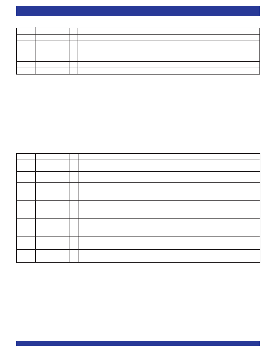
PIN DESCRIPTION (PBGA PACKAGE ONLY)
Symbol
Name
I/O
Description
ASYR(1)
Asynchronous
I
A HIGH on this input during Master Reset will select Synchronous read operation for the output port. A LOW
Read Port
will select Asynchronous operation. If Asynchronous is selected the FIFO must operate in IDT Standard mode.
ASYW(1)
Asynchronous
I
A HIGH on this input during Master Reset will select Synchronous write operation for the input port. A LOW
WritePort
will select Asynchronous operation.
TCK(2)
JTAG Clock
I
Clock input for JTAG function. One of four terminals required by IEEE Standard 1149.1-1990. Test operations of the
device are synchronous to TCK. Data from TMS and TDI are sampled on the rising edge of TCK and outputs change
on the falling edge of TCK. If the JTAG function is not used this signal needs to be tied to GND.
TDI(2)
JTAG Test Data
I
One of four terminals required by IEEE Standard 1149.1-1990. During the JTAG boundary scan operation, test data
Input
seriallyloadedviatheTDIontherisingedgeofTCKtoeithertheInstructionRegister,IDRegisterandBypassRegister.
An internal pull-up resistor forces TDI HIGH if left unconnected.
TDO(2)
JTAG Test Data
O
One of four terminals required by IEEE Standard 1149.1-1990. During the JTAG boundary scan operation, test data
Output
seriallyloadedoutputviatheTDOonthefallingedgeofTCKfromeithertheInstructionRegister,IDRegisterandBypass
Register. This output is high impedance except when shifting, while in SHIFT-DR and SHIFT-IR controller states.
TMS(2)
JTAG Mode
I
TMSisaserialinputpin.OneoffourterminalsrequiredbyIEEEStandard1149.1-1990.TMSdirectsthedevicethrough
its TAP controller states. An internal pull-up resistor forces TMS HIGH if left unconnected.
TRST(2)
JTAG Reset
I
TRST is an asynchronous reset pin for the JTAG controller. The JTAG TAP controller will automatically reset upon
power-up. If the JTAG function is not used then this signal should to be tied to GND.
PIN DESCRIPTION-CONTINUED (TQFP & PBGA PACKAGES)
SEN
Serial Enable
I
SENenablesserialloadingofprogrammableflagoffsets.
WCLK/
WriteClock/
I
If Synchronous operation of the write port has been selected, when enabled by
WEN, the rising edge of WCLK
WR
WriteStrobe
writes data into the FIFO. If Asynchronous operation of the write port has been selected, WR writes data into the FIFO
on a rising edge in an Asynchronous manner, (
WEN should be tied to its active state). Asynchronous operation of
the WCLK/WR input is only available in the PBGA package.
WEN
WriteEnable
I
WEN enables WCLK for writing data into the FIFO memory and offset registers.
VCC
+3.3V Supply
I
These are VCC supply inputs and must be connected to the 3.3V supply rail.
Symbol
Name
I/O
Description
NOTE:
1. Inputs should not change state after Master Reset.
相關PDF資料 |
PDF描述 |
|---|---|
| VI-B7W-MY | CONVERTER MOD DC/DC 5.5V 50W |
| MS27473P20A41P | CONN PLUG 41POS STRAIGHT W/PINS |
| VI-B7V-MY | CONVERTER MOD DC/DC 5.8V 50W |
| VI-26M-IW-S | CONVERTER MOD DC/DC 10V 100W |
| VI-B7T-MY | CONVERTER MOD DC/DC 6.5V 50W |
相關代理商/技術參數(shù) |
參數(shù)描述 |
|---|---|
| IDT72V36110L7-5PF | 功能描述:IC FIFO 131KX36 7-5NS 128QFP RoHS:否 類別:集成電路 (IC) >> 邏輯 - FIFO 系列:72V 標準包裝:15 系列:74F 功能:異步 存儲容量:256(64 x 4) 數(shù)據(jù)速率:- 訪問時間:- 電源電壓:4.5 V ~ 5.5 V 工作溫度:0°C ~ 70°C 安裝類型:通孔 封裝/外殼:24-DIP(0.300",7.62mm) 供應商設備封裝:24-PDIP 包裝:管件 其它名稱:74F433 |
| IDT72V36110L7-5PF8 | 功能描述:IC FIFO 131KX36 7-5NS 128QFP RoHS:否 類別:集成電路 (IC) >> 邏輯 - FIFO 系列:72V 標準包裝:15 系列:74F 功能:異步 存儲容量:256(64 x 4) 數(shù)據(jù)速率:- 訪問時間:- 電源電壓:4.5 V ~ 5.5 V 工作溫度:0°C ~ 70°C 安裝類型:通孔 封裝/外殼:24-DIP(0.300",7.62mm) 供應商設備封裝:24-PDIP 包裝:管件 其它名稱:74F433 |
| IDT72V36110L7-5PFGI | 功能描述:3.3V SUPERSYNC II 36BIT FIFO RoHS:是 類別:集成電路 (IC) >> 邏輯 - FIFO 系列:72V 標準包裝:90 系列:74ABT 功能:同步,雙端口 存儲容量:4.6K(64 x 36 x2) 數(shù)據(jù)速率:67MHz 訪問時間:- 電源電壓:4.5 V ~ 5.5 V 工作溫度:0°C ~ 70°C 安裝類型:表面貼裝 封裝/外殼:120-LQFP 裸露焊盤 供應商設備封裝:120-HLQFP(14x14) 包裝:托盤 產(chǎn)品目錄頁面:1005 (CN2011-ZH PDF) 其它名稱:296-3984 |
| IDT72V36110L7-5PFI | 功能描述:IC FIFO 131KX36 7-5NS 128QFP RoHS:否 類別:集成電路 (IC) >> 邏輯 - FIFO 系列:72V 標準包裝:15 系列:74F 功能:異步 存儲容量:256(64 x 4) 數(shù)據(jù)速率:- 訪問時間:- 電源電壓:4.5 V ~ 5.5 V 工作溫度:0°C ~ 70°C 安裝類型:通孔 封裝/外殼:24-DIP(0.300",7.62mm) 供應商設備封裝:24-PDIP 包裝:管件 其它名稱:74F433 |
| IDT72V3611L12PQF | 制造商:Integrated Device Technology Inc 功能描述:72V3611L12PQF |
發(fā)布緊急采購,3分鐘左右您將得到回復。